(China (Mainland))

Product Summary
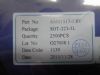
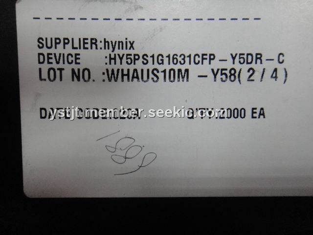
The HY5PS1G1631CFP-Y5DR-C is a 1Gb DDR2 SDRAM.
Parametrics
HY5PS1G1631CFP-Y5DR-C absolute maximum ratings: (1)VDD, Voltage on VDD pin relative to Vss: - 1.0 V ~ 2.3 V; (2)VDDQ, Voltage on VDDQ pin relative to Vss: - 0.5 V ~ 2.3 V; (3)VDDL, Voltage on VDDL pin relative to Vss :- 0.5 V ~ 2.3 V; (4)VIN, VOUT, Voltage on any pin relative to Vss: - 0.5 V ~ 2.3 V; (5)TSTG, Storage Temperature: -55 to +100℃; (6)II, Input leakage current; any input 0V VIN VDD; all other balls not under test = 0V): -2 uA ~ 2 uA; (7)IOZ, Output leakage current; 0V VOUT VDDQ; DQ and ODT disabled: -5 uA ~ 5 uA.
Features
HY5PS1G1631CFP-Y5DR-C features: (1)DM mask write data-in at the both rising and falling edges of the data strobe; (2)All addresses and control inputs except data, data strobes and data masks latched on the rising edges of the clock; (3)Programmable CAS latency 3, 4, 5 and 6 supported; (4)Programmable additive latency 0, 1, 2, 3, 4 and 5 supported; (5)Programmable burst length 4/8 with both nibble sequential and interleave mode; (6)Internal eight bank operations with single pulsed RAS; (7)Auto refresh and self refresh supported; (8)tRAS lockout supported; (9)8K refresh cycles /64ms; (10)JEDEC standard 60ball FBGA(×4/×8) , 84ball FBGA(×16); (11)Full strength driver option controlled by EMRS; (12)On Die Termination supported; (13)Off Chip Driver Impedance Adjustment supported; (14)Read Data Strobe supported (×8 only); (15)Self-Refresh High Temperature Entry.
Diagrams

 |
 HY5PS121621F |
Other |
|
Data Sheet |
Negotiable |
|
||||
|
HY5PS121621FP-C4 |
Other |
|
Data Sheet |
Negotiable |
|
||||
|
HY5PS121621FP-E3 |
Other |
|
Data Sheet |
Negotiable |
|
||||
|
HY5PS121621FP-Y5 |
Other |
|
Data Sheet |
Negotiable |
|
||||
|
HY5PS121621L |
Other |
|
Data Sheet |
Negotiable |
|
||||
|
HY5PS121621LFP-C4 |
Other |
|
Data Sheet |
Negotiable |
|
||||