(China (Mainland))


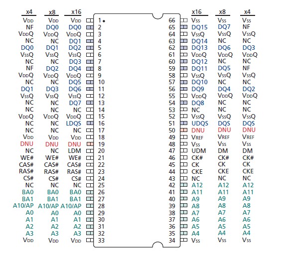
Product Summary
The MT46V64M8P-5BL IT:F is a DDR SDRAM. It operates from a differential clock (CK and CK#); the crossing of CK going HIGH and CK# going LOW will be referred to as the positive edge of CK. Commands (address and control signals) are registered at every positive edge of CK. Input data is registered on both edges of DQS, and output data is referenced to both edges of DQS, as well as to both edges of CK. The MT46V64M8P-5BL IT:F provides for programmable READ or WRITE burst lengths of 2, 4, or 8 locations. An auto precharge function may be enabled to provide a self-timed row precharge that is initiated at the end of the burst access.
Parametrics
MT46V64M8P-5BL IT:F absolute maximum ratings: (1)VDD supply voltage relative to VSS: -1V to 3.6V; (2)VDDQ supply voltage relative to VSS: -1V to 3.6V; (3)VREF and inputs voltage relative to VSS: -1V to 3.6V; (4)I/O pins voltage relative to VSS: -0.5V VDDQ + 0.5V V; (5)Storage temperature (plastic): -55 to 150 °C; (6)Short circuit output current: -50 mA.
Features
MT46V64M8P-5BL IT:F features: (1)Bidirectional data strobe (DQS) transmitted/; (2)received with data, i.e., source-synchronous data; (3)capture (x16 has two-one per byte); (4)Internal, pipelined double-data-rate (DDR) architecture; two data accesses per clock cycle; (5)Differential clock inputs (CK and CK#); (6)Commands entered on each positive CK edge; (7)DQS edge-aligned with data for READs; centeraligned with data for WRITEs; (8)DLL to align DQ and DQS transitions with CK; (9)Four internal banks for concurrent operation; (10)Data mask (DM) for masking write data (x16 has two - one per byte); (11)Programmable burst lengths: 2, 4, or 8; (12)Auto refresh-64ms, 8192-cycle; (13)Longer-lead TSOP for improved reliability (OCPL); (14)2.5V I/O (SSTL_2 compatible); (15)Concurrent auto precharge option is supported.
Diagrams