(China (Mainland))

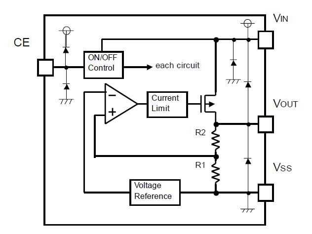
Product Summary
The XC6219B121MR is a highly accurate, low noise, CMOS LDO Voltage Regulator. Offering low output noise, high ripple rejection ratio, low dropout and very fast turn-on times, the XC6219B121MR is ideal for today’s cutting edge mobile phone. Internally the XC6219B121MR includes a reference voltage source, error amplifiers, driver transistors, current limiters and phase compensators.
Parametrics
XC6219B121MR absolute maximum ratings: (1)Input Voltage, VIN: 7.0 V; (2)Output Current, IOUT: 500 mA; (3)Output Voltage, VOUT: VSS -0.3 to VIN + 0.3 V; (4)CE Pin Voltage, VCE: VSS -0.3 to VIN + 0.3 V; (5)Power Dissipation, SOT-25, Pd: 250mW; SOT-89, Pd: 500mW; USP-6B, Pd: 100mW; (6)Operating Temperature Range, Topr: -40 to +85℃; (7)Storage Temperature Range, Tstg: -55 to +125℃.
Features
XC6219B121MR features: (1)Maximum Output Current 150mA (VOUT<1.75V); 240mA (VOUT>1.8V); (300mA limit (TYP)); (2)Dropout Voltage 200mV (IOUT=100mA); (3)Operating Voltage Range 2.0V ~ 6.0V; (4)Output Voltage Range 0.9V ~ 5.0V (50mV steps); (5)Highly Accurate + 2% (VOUT>1.5V).
Diagrams