Product Summary
The EM6AA160TSA-5G is a high-speed CMOS double data rate synchronous DRAM containing 256 Mbits. It is internally configured as a quad 4M x 16 DRAM with a synchronous interface (all signals are registered on the positive edge of the clock signal, CK). Data outputs occur at both rising edges of CK and CK .d Read and write accesses to the SDRAM are burst oriented; accesses start at a selected location and continue for a programmed number of locations in a programmed sequence. Accesses begin with the registration of a BankActivate command which is then followed by a Read or Write command. The EM6AA160TSA-5G provides programmable Read or Write burst lengths of 2, 4, or 8. An auto precharge function may be enabled to provide a self-timed row precharge that is initiated at the end of the burst sequence. The refresh functions, either Auto or Self Refresh are easy to use. In addition, the EM6AA160TSA-5G features programmable DLL option. By having a programmable mode register and extended mode register, the system can choose the most suitable modes to maximize its performance. The EM6AA160TSA-5G is well suited for applications requiring high memory bandwidth, result in a device particularly well suited to high performance main memory and graphics applications.
Parametrics
EM6AA160TSA-5G absolute maximum ratings: (1)VIN, VOUT Input, Output Voltage: - 0.5~ VDDQ + 0.5 V; (2)VDD, VDDQ Power Supply Voltage: 1~3.6 V; (3)TA Ambient Temperature: 0~70 °C; (4)TSTG Storage Temperature: - 65~150 °C; (5)TSOLDER Soldering Temperature: 260 °C; (6)PD Power Dissipation: 1 W; (7)IOUT Short Circuit Output Current: 50 mA.
Features
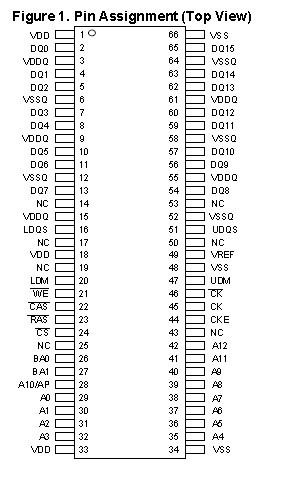
EM6AA160TSA-5G features: (1)Fast clock rate: 250/200MHz; (2)Differential Clock CK & CK; (3)Bi-directional DQS; (4)DLL enable/disable by EMRS; (5)Fully synchronous operation; (6)Internal pipeline architecture; (7)Four internal banks, 4M x 16-bit for each bank; (8)Programmable Mode and Extended Mode registers: CAS Latency: 2.5, 3; Burst length: 2, 4, 8; (9)- Burst Type: Sequential & Interleaved; (10)Individual byte write mask control; (11)DM Write Latency = 0; (12)Auto Refresh and Self Refresh; (13)8192 refresh cycles / 64ms; (14)Precharge & active power down; (15)Power supplies: VDD & VDDQ = 2.5V ± 5%; (16)Interface: SSTL_2 I/O Interface; (17)Package: 66 Pin TSOP II, 0.65mm pin pitch: Pb free and Halogen free.
Diagrams

 (China (Mainland))


