Product Summary
The GS8182Q18BGD-200 is a 18Mb Burst of 2 SigmaQuad-II SRAM. The GS8182Q18BGD-200 is built in compliance with the SigmaQuad-II SRAM pinout standard for Separate I/O synchronous SRAMs. The device is 18,874,368-bit (18Mb) SRAMs. The device is the first in a family of wide, very low voltage HSTL I/O SRAMs designed to operate at the speeds needed to implement economical high performance networking systems.
Parametrics
GS8182Q18BGD-200 absolute maximum ratings: (1)VDD Voltage on VDD Pins: -0.5 to 2.9 V; (2)VDDQ Voltage in VDDQ Pins: -0.5 to VDD V; (3)VREF Voltage in VREF Pins: -0.5 to VDDQ V; (4)VI/O Voltage on I/O Pins: -0.5 to VDDQ +0.5 (≤ 2.9 V max.) V; (5)VIN Voltage on Other Input Pins: -0.5 to VDDQ +0.5 (≤ 2.9 V max.) V; (6)IIN Input Current on Any Pin: +/–100 mA dc; (7)IOUT Output Current on Any I/O Pin: +/–100 mA dc; (8)TJ Maximum Junction Temperature: 125℃; (9)TSTG Storage Temperature: -55 to 125℃.
Features
GS8182Q18BGD-200 features: (1)Simultaneous Read and Write SigmaQuad?Interface; (2)JEDEC-standard pinout and package; (3)Dual Double Data Rate interface; (4)Byte Write controls sampled at data-in time; (5)Burst of 2 Read and Write; (6)1.8 V +150/-100 mV core power supply; (7)1.5 V or 1.8 V HSTL Interface; (8)Pipelined read operation; (9)Fully coherent read and write pipelines; (10)ZQ mode pin for programmable output drive strength; (11)IEEE 1149.1 JTAG-compliant Boundary Scan; (12)165-bump, 13 mm x 15 mm, 1 mm bump pitch BGA package; (13)Pin-compatible with future 36Mb, 72Mb, and 144Mb devices.
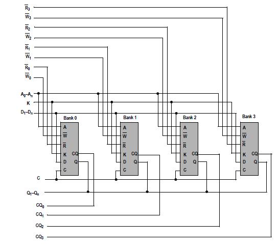
Diagrams

 (China (Mainland))


