(China (Mainland))


Product Summary
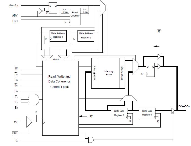
The GS880Z36BT-250 is a 9Mbit Synchronous Static SRAM. GSI’s NBT SRAMs, like ZBT, NtRAM, NoBL or other pipelined read/double late write or flow through read/single late write SRAMs, allow utilization of all available bus bandwidth by eliminating the need to insert deselect cycles when the device is switched from read to write cycles. Because the GS880Z36BT-250 is a synchronous device, address, data inputs, and read/ write control inputs are captured on the rising edge of the input clock.
Parametrics
GS880Z36BT-250 absolute maximum ratings: (1)VDD, Voltage on VDD Pins: -0.5 to 4.6 V; (2)VDDQ, Voltage in VDDQ Pins: -0.5 to 4.6 V; (3)VI/O, Voltage on I/O Pins: -0.5 to VDDQ +0.5 (≤ 4.6 V max.) V; (4)VIN, Voltage on Other Input Pins: -0.5 to VDD +0.5 (≤ 4.6 V max.) V; (5)IIN, Input Current on Any Pin: +/–20 mA; (6)IOUT, Output Current on Any I/O Pin: +/–20 mA; (7)PD, Package Power Dissipation: 1.5 W; (8)TSTG, Storage Temperature: -55 to 125℃; (9)TBIAS, Temperature Under Bias: -55 to 125℃.
Features
GS880Z36BT-250 features: (1)NBT (No Bus Turn Around) functionality allows zero wait read-write-read bus utilization; Fully pin-compatible with both pipelined and flow through NtRAM NoBL and ZBT-SRAMs; (2)2.5 V or 3.3 V +10%/?0% core power supply; (3)2.5 V or 3.3 V I/O supply; (4)User-configurable Pipeline and Flow Through mode; (5)LBO pin for Linear or Interleave Burst mode; (6)Pin compatible with 2M, 4M, and 18M devices; (7)Byte write operation (9-bit Bytes); (8)3 chip enable signals for easy depth expansion; (9)ZZ Pin for automatic power-down; (10)JEDEC-standard 100-lead TQFP package; (11)Pb-Free 100-lead TQFP package available.
Diagrams