(China (Mainland))


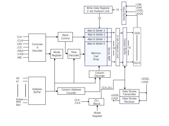
Product Summary
The H5DU2562GFR-J3C is a 268,435,456-bit CMOS Double Data Rate(DDR) Synchronous DRAM. The H5DU2562GFR-J3C is ideally suited for the main memory applications which requires large memory density and high bandwidth. The H5DU2562GFR-J3C DDR SDRAMs offer fully synchronous operations referenced to both rising and falling edges of the clock.
Parametrics
H5DU2562GFR-J3C absolute maximum ratings: (1) Operating Temperature (Ambient) TA: -40 to 85°C; (2) Storage Temperature TSTG: -55 to 150°C; (3) Voltage on VDD relative to VSS, VDD: -1 to 3.6V; (4) Voltage on V DDQ relative to VSS, VDDQ: -1 to 3.6V; (5) Voltage on inputs relative to VSS, VINPUT: -1 to 3.6V; (6) Voltage on I/O pins relative to VSS, VIO: -0.5 to 3.6V; (7) Output Short Circuit Current IOS: 50mA; (8) Soldering Temperature Time TSOLDER: 260°C, 10 sec.
Features
H5DU2562GFR-J3C features: (1) VDD, VDDQ = 2.5V +/- 0.2V; (2) All inputs and outputs are compatible with SSTL_2 interface; (3) Fully differential clock inputs (CK, /CK) operation; (4) Double data rate interface; (5) Source synchronous -data transaction aligned to bidirectional data strobe (DQS) ; (6) DM mask write data-in at the both rising and falling edges of the data strobe; (7) Auto refresh and self refresh supported; (8) tRAS lock out function supported; (9) 8192 refresh cycles/64ms; (10) 60 Ball FBGA Package Type.
Diagrams