(China (Mainland))

Product Summary
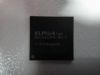
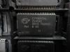
The HDMP-0421 is a Single Port Bypass Circuit (PBC) with Clock and Data Recovery (CDR), and dual Signal Detect (SD) capability. This configuration will control jitter accumulation while repeating incoming signals. Port Bypass Circuits are used to provide loops that are continuously on in hard disk arrays constructed in Fibre Channel Arbitrated Loop (FC-AL) configurations. Hard disks may be pulled out or swapped while other disks in the array are available to the system. This device may also be used in multi-initiator loop configurations. The applications of the HDMP-0421 include RAID, JBOD Cabinets, 1=>1 Gigabit Serial Buffer Pair (with and w/o CDR), Multi-Initiator Loops.
Parametrics
HDMP-0421G absolute maximum ratings: (1)VCC, Supply Voltage: -0.7 to 4.0V; (2)VIN,LVTTL, LVTTL Input Voltage: -0.7 to 4.0; (3)VIN,HS_IN, HS_IN Input Voltage: 2.0 VCC; (4)IO,LVTTL, LVTTL Output Source Current: ±13mA; (5)Tstg, Storage Temperature: -65 to +150℃; (6)Tj, Junction Temperature: 0 to +125℃.
Features
HDMP-0421G features: (1)Supports ANSI X3T11 1.0625 Gbps FC-AL Loop Configuration; (2)Supports 802.3z 1.25 Gbps Gigabit Ethernet (GE) Rates; (3)Single PBC, CDR, Dual Signal Detect (SD) in a Single Package; (4)Bidirectional, Symmetric Bypass Capability; (5)CDR in Bypass Path and Loop Path; (6)CDR Location Determined by Wiring Configuration of Pins on PCB (Patent Pending); (7)Envelope Detect on Cable Input (SD) for Both Directions; (8)Equalizers On All Inputs; (9)High Speed PECL I/Os Referenced to VCC; (10)Buffered Line Logic (BLL) Outputs without External Bias Resistors; (11)0.4 W Typical Po.
Diagrams