(China (Mainland))

Product Summary
The K4B4G0446B-HYK0 DDP 4Gb B-die DDR3 SDRAM is organized as a 128Mbit x 4 I/Os x 8banks, 64Mbit x 8 I/Os x 8banks device. The K4B4G0446B-HYK0 achieves high speed double-data-rate transfer rates of up to 1333Mb/sec/pin (DDR3-1600) for general applications. The chip is designed to comply with the following key DDR3 SDRAM features such as posted CAS, Programmable CWL, Internal (Self) Calibration, On Die Termination using ODT pin and Asynchronous Reset. All of the control and address inputs are synchronized with a pair of externally supplied differential clocks. Inputs are latched at the crosspoint of differential clocks (CK rising and CK falling).
Parametrics
K4B4G0446B-HYK0 absolute maximum ratings: (1)VDD, Voltage on VDD pin relative to Vss: -0.4V to 1.975V; (2)VDDQ, Voltage on VDDQ pin relative to Vss: -0.4V to 1.975V; (3)VIN, VOUT, Voltage on any pin relative to Vss: -0.4V to 1.975V; (4)TSTG, Storage Temperature: -55 to +100℃.
Features
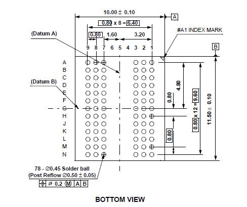
K4B4G0446B-HYK0 features: (1)JEDEC standard 1.5V -0.075V Power Supply; (2)VDDQ = 1.5V -0.075V; (3)400 MHz fCK for 800Mb/sec/pin, 533MHz fCK for 1066Mb/sec/pin, 667MHz fCK for 1333Mb/sec/pin; (4)8 Banks; (5)Posted CAS; (6)Programmable CAS Latency(posted CAS): 6, 7, 8, 9, 10; (7)Programmable Additive Latency: 0, CL-2 or CL-1 clock; (8)Programmable CAS Write Latency (CWL) = 5 (DDR3-800), 6 (DDR3-1066) and 7 (DDR3-1333); (9)8-bit pre-fetch; (10)Burst Length: 8 (Interleave without any limit, sequential with starting address "000" only), 4 with tCCD = 4 which does not allow seamless read or write [either On the fly using A12 or MRS]; (11)Bi-directional Differential Data-Strobe; (12)Internal(self) calibration : Internal self calibration through ZQ pin (RZQ : 240 ohm ±1%); (13)On Die Termination using ODT pin; (14)Average Refresh Period 7.8us at lower than TCASE 85℃, 3.9us at 85℃ < TCASE < 95℃; (15)Asynchronous Reset; (16)Package: 78 balls FBGA - x4/x8; (17)All of Lead-Free products are compliant for RoHS; (18)All of products are Halogen-free.
Diagrams