Product Summary
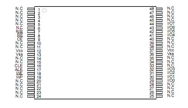
The K9F1208U0C-PCB0 is a 528Mbits (553,648,218 bits) memory organized as 131,072 rows (pages) by 528 columns. The K9F1208U0C-PCB0 array is made up of 16 cells that are serially connected to form a NAND structure. It indicates that the bit by bit erase operation is prohibited on the K9F1208U0C-PCB0. A NAND structure of the K9F1208U0C-PCB0 consists of 16 cells. Total 135,168 NAND structures reside in a block.
Parametrics
K9F1208U0C-PCB0 absolute maximum ratings: (1) Voltage on any pin relative to VSS VCC: -0.6V to +2.45V (1.8V Device) , -0.6V to +4.6V (2.7V/3.3V Device) , VIN: -0.6V to +2.45V (1.8V Device) , -0.6V to +4.6V (2.7V/3.3V Device) , VI/O: -0.6V to VCC +0.3V (1.8V Device) , -0.6V to VCC +0.3V (2.7V/3.3V Device); (3) Storage Temperature Tstg: -65°C to +150°C; (4) Short Circuit Current IOS: 5mA.
Features
K9F1208U0C-PCB0 features: (1) Memory Cell Array : (64M + 2M) x 8bits; (2) Automatic Program and Erase; (3) Block Erase : (16K + 512)Bytes; (4) Block Erase : (16K + 512)Bytes; (5) Program/Erase Lockout During Power Transitions; (6) Reliable CMOS Floating-Gate Technology; (7) Command Register Operation; (8) Unique ID for Copyright Protection.
Diagrams

 |
 K9F1208D0A |
 Other |
 |
 Data Sheet |
 Negotiable |
|
||||
 |
 K9F1208Q0A-XXB0 |
 Other |
 |
 Data Sheet |
 Negotiable |
|
||||
 |
 K9F1208Q0B |
 Other |
 |
 Data Sheet |
 Negotiable |
|
||||
 |
 K9F1208R0B |
 Other |
 |
 Data Sheet |
 Negotiable |
|
||||
 |
 K9F1208U0A |
 Other |
 |
 Data Sheet |
 Negotiable |
|
||||
 |
 K9F1208U0A-VCB0 |
 Other |
 |
 Data Sheet |
 Negotiable |
|
||||
 (China (Mainland))


