(China (Mainland))

Product Summary
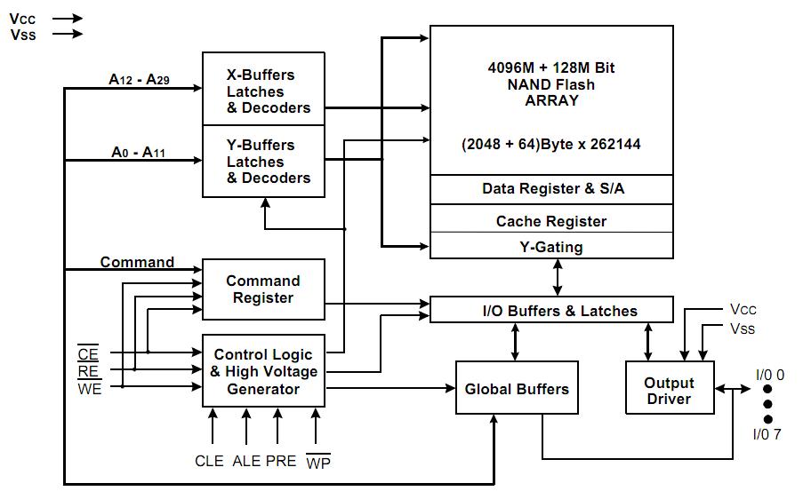
The K9K4G08UOM-PCBO is a 512Mx8bit or 256Mx16bit NAND Flash Memory. The K9K4G08UOM-PCBO’s NAND cell provides the most cost-effective solution for the solid state mass storage market. A program operation can be performed in typical 300ms on the 2112-byte(X8 device) or 1056-word(X16 device) page and an erase operation can be performed in typical 2ms on a 128K-byte(X8 device) or 64K-word(X16 device) block. Data in the data page can be read out at 50ns cycle time per byte (30ns, only X8 3.3v device) or word(X16 device). The I/O pins serve as the ports for address and data input/output as well as command input.
Parametrics
K9K4G08UOM-PCBO absolut maximum ratings: (1)Voltage on any pin relative to VSS, VCC: -0.6 to +4.6V; VIN: -0.6 to +4.6V; VI/O: -0.6 to Vcc+0.3V; (2)Temperature Under Bias, TBIAS: -10 to +125℃; (3)Storage Temperature, TSTG: -65 to +150℃; (4)Short Circuit Current, IOS: 5mA.
Features
K9K4G08UOM-PCBO features: (1)Fast Write Cycle Time, Program time: 300ms(Typ.); Block Erase Time: 2ms(Typ.); (2)Command/Address/Data Multiplexed I/O Port; (3)Hardware Data Protection, Program/Erase Lockout During Power Transitions; (4)Reliable CMOS Floating-Gate Technology, Endurance : 100K Program/Erase Cycles; Data Retention: 10 Years; (5)Command Register Operation; (6)Cache Program Operation for High Performance Program; (7)Power-On Auto-Read Operation; (8)Intelligent Copy-Back Operation; (9)Unique ID for Copyright Protection; (10)Package: K9XXGXXXXM-YCB0/YIB0, 48 - Pin TSOP I (12 x 20 / 0.5 mm pitch); K9W8G08U1M-YCB0/YIB0: Two K9K4G08U0M stacked; 48 - Pin TSOP I (12 x 20 / 0.5 mm pitch); K9XXGXXXXM-PCB0/PIB0, 48 - Pin TSOP I (12 x 20 / 0.5 mm pitch); K9W8G08U1M-PCB0/PIB0: Two K9K4G08U0M stacked, 48 - Pin TSOP I (12 x 20 / 0.5 mm pitch).
Diagrams