(China (Mainland))

Product Summary
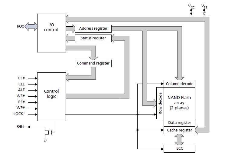
The MT29F84G08AMCABH2-12Q:A is a micron NAND Flash device. It include an asynchronous data interface for high-performance I/O operations. The MT29F84G08AMCABH2-12Q:A use a highly multiplexed 8-bit bus (I/Ox) to transfer commands, address, and data. The MT29F84G08AMCABH2-12Q:A five control signals used to implement the asynchronous data interface: CE#, CLE, ALE, WE#, and RE#. Additional signals control hardware write protection and monitor device status (R/B#). This hardware interface creates a low pin-count device with a standard pinout that remains the same from one density to another, enabling future upgrades to higher densities with no board redesign. A target is the unit of memory accessed by a chip enable signal. A target contains one or more NAND Flash die. The MT29F84G08AMCABH2-12Q:A die is the minimum unit that can independently execute commands and report status. The MT29F84G08AMCABH2-12Q:A die, in the ONFI specification, is referred to as a logical unit (LUN). There is at least one NAND Flash die per chip enable signal. For further details, see device and array organization. This device has an internal 4-bit ECC that can be enabled using the GET/SET features. See internal ECC and spare area mapping for ECC for more information.
Parametrics
MT29F84G08AMCABH2-12Q:A absolute maximum ratings: (1)Voltage input, 1.8V, VIN: –0.6 to 2.4 V; 3.3V, VIN: –0.6 to 4.6 V; (2)VCC supply voltage, 1.8V, VCC: –0.6 to 2.4 V; 3.3V, VCC: –0.6 to 4.6 V; (3)Storage temperature, TSTG: –65 to 150 °C; (4)Short circuit output current, I/Os: 5 mA.
Features
MT29F84G08AMCABH2-12Q:A features: (1)Open NAND flash interface (ONFI)1.0-compliant1; (2)Single-level cell (SLC)technology; (3)Organization: Page size x8: 2112 bytes (2048 + 64 bytes); Page size x16: 1056 words (1024 + 32 words); Block size: 64 pages (128K + 4K bytes); Plane size: 2 planes x 2048 blocks per plane; Device size: 4Gb: 4096 blocks; 8Gb: 8192 blocks 16Gb: 16,384 blocks; (4)Asynchronous I/O performance: tRC/tWC: 20ns (3.3V), 25ns (1.8V); (5)Array performance: Read page: 25μs; Program page: 200μs (TYP: 1.8V, 3.3V); Erase block: 700μs (TYP); (6)Command set: ONFI NAND Flash Protocol; (7)Advanced command set: Program page cache mode; Read page cache mode; One-time programmable (OTP)mode; Two-plane commands; Interleaved die (LUN)operations; Read unique ID; Block lock (1.8V only); Internal data move.
Diagrams