(China (Mainland))

Product Summary
The MT47H128M16HG-3IT is a DDR2 SDRAM. The MT47H128M16HG-3IT operates from a differential clock (CK and CK#); the crossing of CK going HIGH and CK# going LOW will be referred to as the positive edge of CK. Commands (address and control signals) are registered at every positive edge of CK. Input data is registered on both edges of DQS, and output data is referenced to both edges of DQS as well as to both edges of CK. It provides for programmable read or write burst lengths of four or eight locations. The MT47H128M16HG-3IT supports interrupting a burst read of eight with another read or a burst write of eight with another write. An auto precharge function may be enabled to provide a self-timed row precharge that is initiated at the end of the burst access.
Parametrics
MT47H128M16HG-3IT absolute maximum ratings: (1)VDD supply voltage relative to VSS: -1V to +2.3V; (2)VDDQ supply voltage relative to VSSQ: -0.5 to +2.3V; (3)VDDL supply voltage relative to VSSL: -0.5 to +2.3V; (4)Voltage on any ball relative to VSS: -0.5 to +2.3V; (5)Input leakage current: -5 to 5 uA; (6)Output leakage current: -5 to 5 uA; (7)VREF leakage current; VREF = valid VREF level: -2 to 2 uA.
Features
MT47H128M16HG-3IT features: (1)VDD = 1.8V +/-0.1V, VDDQ = 1.8V+/-0.1V; (2)JEDEC-standard 1.8V I/O (SSTL_18-compatible); (3)Differential data strobe (DQS, DQS#) option; (4)4n-bit prefetch architecture; (5)Duplicate output strobe (RDQS) option for x8; (6)DLL to align DQ and DQS transitions with CK; (7)8 internal banks for concurrent operation; (8)Programmable CAS latency (CL); (9)Posted CAS additive latency (AL); (10)WRITE latency = READ latency - 1 tCK; (11)Programmable burst lengths: 4 or 8; (12)Adjustable data-output drive strength; (13)64ms, 8192-cycle refresh; (14)On-die termination (ODT); (15)Industrial temperature (IT) option; (16)RoHS-compliant; (17)Supports JEDEC clock jitter specification.
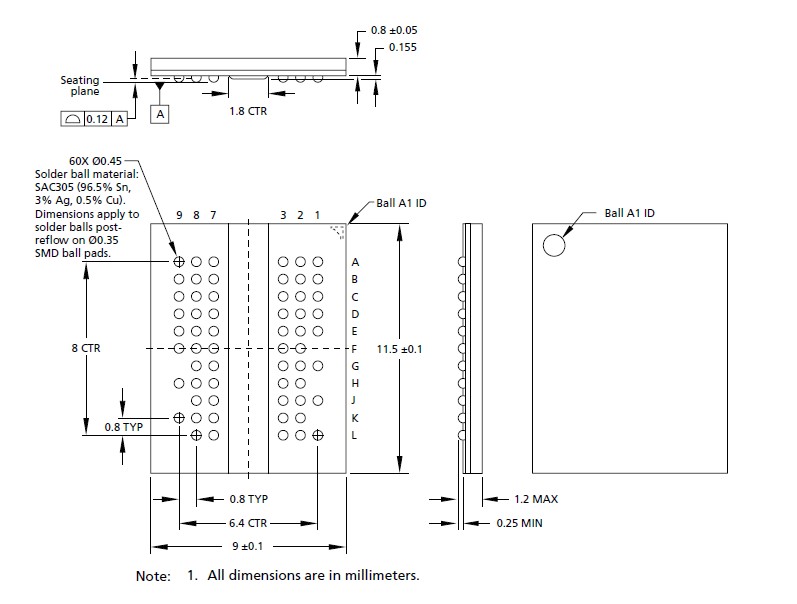
Diagrams