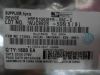
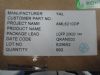
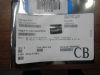
(China (Mainland))

Product Summary
The PI74SSTUA is a 25-Bit 1:1 or 14-Bit 1:2 configurable registered buffer and designed for 1.7V to 1.9V VDD operation. All clock and data inputs are compatible with the JEDEC standard for SSTL_18. The control inputs are LVCMOS. All outputs are 1.8V drivers that have been optimized to drive the DDR2 DIMM load, and meet SSTL_18 specifi cations.
Parametrics
PI74SSTUA absolute maximum ratings: (1)Storage Temperature: -65℃ to +150℃; (2)Supply Voltage Range, VDD: -0.5V to 2.5V; (3)Input Voltage Range, VI: -0.5V to 2.5V; (4)Output Voltage Range, VO: -0.5V to VDD + 0.5V; (5)Input Clamp Current, IIK (VI < 0 or VI = VDD): -50mA; (6)Output Clamp Current, IOK (VO < 0 or VO > VDD): ±50mA; (7)Continous Output Current, IO (VO = 0 to VDD): ±50mA; (8)Continous Current through each VDD or GND: ±100mA.
Features
PI74SSTUA features: (1)Designed for low-voltage operation: VDD = 1.8V; (2)Supports Low Power Standby Operation; (3)Enhanced Signal Integrity for 1 and 2 Rank Modules; (4)All Inputs are SSTL_18 compatible, except RST, C0, C1, which are LVCMOS; (5)Output drivers are optimized to drive DDR2 DIMM loads; (6)Packaging (Pb-free & Green available): 96-Ball LFBGA (NB); (7)Used in DDR2-400/533/667 memory applications.
Diagrams