(China (Mainland))

Product Summary
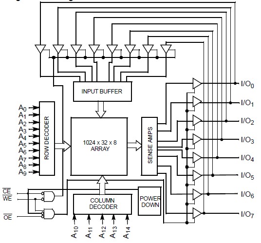
The CY7C199-20VI is a high-performance CMOS static RAM organized as 32,768 words by 8 bits. Easy memory expansion is provided by an active low chip enable (CE) and active low output enable (OE) and three-state drivers. The CY7C199-20VI has an automatic power-down feature, reducing the power consumption by 81% when deselected. The CY7C199-20VI is in the standard 300-mil-wide DIP, SOJ, and LCC packages. An active LOW Write Enable signal (WE) controls the writing/reading operation of the memory. When CE and WE inputs are both LOW, data on the eight data input/output pins (I/O0 through I/O7) is written into the memory location addressed by the address present on the address pins (A0 through A14). Reading the CY7C199-20VI is accomplished by selecting the device and enabling the outputs, CE and OE active LOW, while WE remains inactive or HIGH. Under these conditions, the contents of the location addressed by the information on address pins are present on the eight data input/output pins. The input/output pins remain in a high-impedance state unless the chip is selected, outputs are enabled, and Write Enable (WE) is HIGH. A die coat is used to improve alpha immunity.
Parametrics
CY7C199-20VI absolute maximum ratings: (1)Storage temperature: –65°C to +150°C; (2)Ambient temperature with power applied: –55°C to +125°C; (3)Supply voltage to ground potential (pin 28 to pin 14): –0.5V to +7.0V; (4)DC voltage applied to outputs in high-z state[1]: –0.5V to VCC + 0.5V; (5)DC input voltage[1]: –0.5V to VCC + 0.5V; (6)Output current into outputs (LOW): 20 mA; (7)Static discharge voltage: > 2001V (per MIL-STD-883, Method 3015); (8)Latch-up current: > 200 mA.
Features
CY7C199-20VI features: (1)High speed: 10 ns; (2)Fast tDOE; (3)CMOS for optimum speed/power; (4)Low active power: 467 mW (max, 12 ns “L” version); (5)Low standby power: 0.275 mW (max, “L” version); (6)2V data retention (“L” version only); (7)Easy memory expansion with CE and OE features; (8)TTL-compatible inputs and outputs; (9)Automatic power-down when deselected.
Diagrams