(China (Mainland))


Product Summary
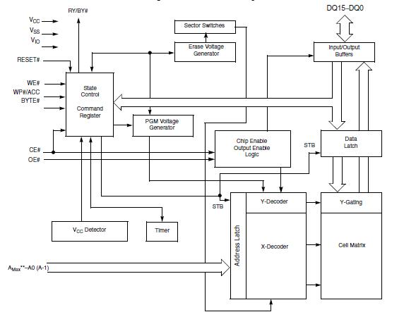
The GL512P10FFSS is a 3.0 Volt-only Page Mode Flash Memory fabricated on 90 nm process technology. The device offers a fast page access time of 25 ns with a corresponding random access time as fast as 90 ns. They feature a Write Buffer that allows a maximum of 32 words/64 bytes to be programmed in one operation, resulting in faster effective programming time than standard programming algorithms. This makes the device ideal for today’s embedded applications that require higher density, better performance and lower power consumption.
Parametrics
GL512P10FFSS absolute maximum ratings: (1)Storage Temperature, Plastic Packages: -65 to +150℃; (2)Ambient Temperature with Power Applied: -65 to +125℃; (3)Voltage with Respect to Ground, All Inputs and I/Os except as noted below: -0.5 V to VCC + 0.5 V; VCC: -0.5 V to +4.0 V; VIO: -0.5V to +4.0V; (4)A9 and ACC: -0.5 V to +12.5 V; (5)Output Short Circuit Current: 200 mA.
Features
GL512P10FFSS features: (1)Single 3V read/program/erase (2.7-3.6 V); (2)Enhanced VersatileI/O. control, All input levels (address, control, and DQ input levels) and outputs are determined by voltage on VIO input. VIO range is 1.65 to VCC; (3)90 nm MirrorBit process technology; (4)8-word/16-byte page read buffer; (5)32-word/64-byte write buffer reduces overall programming time for multiple-word updates Secured Silicon Sector region, 128-word/256-byte sector for permanent, secure identification through an 8-word/16-byte random Electronic Serial Number; Can be programmed and locked at the factory or by the customer; (6)Uniform 64Kword/128KByte Sector Architecture: Five hundred twelve sectors; (7)100,000 erase cycles per sector typical; (8)20-year data retention typical.
Diagrams