(China (Mainland))

Product Summary
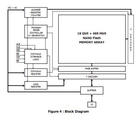
The H27S1G8F2BFR-Bi is a 2048Mx8bit NAND Flash with spare 116Mx8 bit capacity. The H27S1G8F2BFR-Bi is offered with 3.3V Vcc Core Power Supply and 3.3V Input-Output Power Supply. Its NAND cell provides the most cost-effective solution for the solid state mass storage market. The memory is divided into blocks that can be erased independently so it is possible to preserve valid data while old data is erased. The H27S1G8F2BFR-Bi contains 4096 blocks, composed by 128 pages consisting in two NAND structures of 32 series connected Flash cells. Every cell holds two bits. The H27S1G8F2BFR-Bi includes also extra Features like OTP/Unique ID area, Read ID2 extension. The H27S1G8F2BFR-Bi is available in the following packages: TSOP48 (12x20).
Parametrics
H27S1G8F2BFR-Bi absolute maximum ratings: (1)TA, Ambient Operating Temperature (Commercial Temperature Range): 0 to 70℃; Ambient Operating Temperature (Extended Temperature Range): -25 to 85℃; (2) Ambient Operating Temperature (Industrial Temperature Range): -40 to 85℃; (3)TBIAS Temperature Under Bias: -50 to 125℃; (4)TSTG Storage Temperature: -65 to 150℃; (5)VIO Input or Output Voltage: -0.6 to 4.6 V; (6)VCC Supply Voltage: -0.6 to 4.6 V.
Features
H27S1G8F2BFR-Bi features: (1)high density nand flash memories: cost effective solutions for mass storage applications; (2)multiplane architecture: array is split into two independent planes. Parrallel operations on both planes are avaliable, halving program, read and erase time; (3)nand interface: ×8 bus width; address/data multiplexing; pin-out compatibility for all densities; (4)suply voltage: 3.3V device: VCC=2.7V to 3.6V; (5)memory cell array: _4k+224) bytes×128pages×4096blocks.
Diagrams