(China (Mainland))

Product Summary
The H5GQ1H24AFR-T2C is a 1Gb (32Mx32) GDDR5 SGRAM. Read and write accesses to the GDDR5 SGRAM are burst oriented; an access starts at a selected location and consists of a total of eight data words. Accesses begin with the registration of an ACTIVE command, which is then followed by a READ or WRITE command. The H5GQ1H24AFR-T2C uses a 8n prefetch architecture and DDR interface to achieve highspeed operation. The device can be configured to operate in x32 mode or x16 (clamshell) mode. The mode is detected during device initialization.
Parametrics
H5GQ1H24AFR-T2C absolute maximum ratings: (1)Voltage on Vdd Supply Relative to Vss: -0.5 to +2.0 V; (2)Voltage on VddQ Supply Relative to Vss: -0.5 to 2.0 V; (3)Voltage on Vref and Inputs Relative to Vss: -0.5 to 2.0 V; (4)Storage Temperature: -55 to +150°C; (5)Short Circuit Output Current: 50mA.
Features
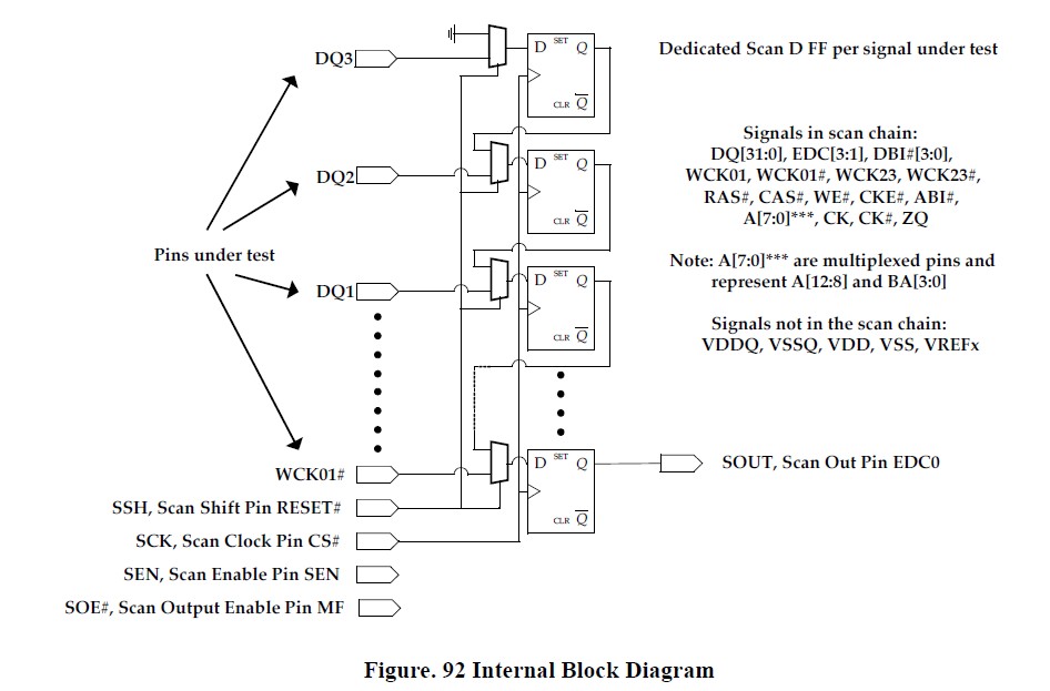
H5GQ1H24AFR-T2C features: (1)Single ended interface for data, address and command; (2)Quarter data]rate differential clock inputs CK/CK# for ADR/CMD; (3)Two half data]rate differential clock inputs WCK/ WCK#, each associated with two data bytes (DQ, DBI#, EDC); (4)Double Data Rate (DDR) data (WCK); (5)Single Data Rate (SDR) command (CK); (6)Double Data Rate (DDR) addressing (CK); (7)16 internal banks; (8)4 bank groups for tCCDL = 3 tCK . 8n prefetch architecture: 256 bit per array read or write access; (9)Burst length: 8 only; (10)Programmable CAS latency: 5 to 20 tCK; (11)Programmable WRITE latency: 1 to 7 tCK; (12)WRITE Data mask function via address bus (single/ double byte mask); (13)Data bus inversion (DBI) & address bus inversion (ABI); (14)Input/output PLL on/off mode; (15)Address training: address input monitoring by DQ pins; (16)WCK2CK clock training with phase information by EDC pins; (17)Data read and write training via READ FIFO; (18)READ FIFO pattern preload by LDFF command; (19)Direct write data load to READ FIFO by WRTR command; (20)Programmable termination and driver strength offsets; (21)Selectable external or internal VREF for data inputs; programmable offsets for internal VREF; (22)Separate external VREF for address / command inputs; (23)Vendor ID, FIFO depth and Density info fields for identification; (24)x32/x16 mode configuration set at power]up with EDC pin; (25)Mirror function with MF pin; (26)Boundary scan function with SEN pin; (27)1.6V / 1.5V +/0.045V supply for device operation (VDD); (28)1.6V / 1.5V +/0.045V supply for I/O interface (VDDQ); (29)170 ball BGA package.
Diagrams