Product Summary
The H5MS1G22MFR-J3M is a 1,073,741,824-bit CMOS Low Power Double Data Rate Synchronous DRAM. It is ideally suited for mobile applications which use the battery such as PDAs, 2.5G and 3G cellular phones with internet access and multimedia capabilities, mini-notebook, hand-held PCs. It is organized as 4banks of 8,388,608 x32. The H5MS1G22MFR-J3M provides for programmable read or write bursts of 2, 4 or 8 locations. An AUTO PRECHARGE function may be enabled to provide a self-timed row precharge that is initiated at the end of the burst access. It also provides for special programmable Self Refresh options which are Partial Array Self Refresh (full, half, quarter and 1/8 and 1/16 array) and Temperature Compensated Self Refresh.
Parametrics
H5MS1G22MFR-J3M absolute maximum ratings: (1)Operating Case Temperature: -30 to 85 °C; (2)Storage Temperature: -55 to 150°C; (3)Voltage on Any Pin relative to VSS: -0.3 to VDDQ+0.3 V; (4)Voltage on VDD relative to VSS: -0.3 to 2.7 V; (5)Voltage on VDDQ relative to VSS: -0.3 to 2.7 V; (6)Short Circuit Output Current: 50 mA; (7)Power Dissipation: 0.7 W.
Features
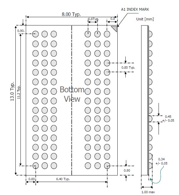
H5MS1G22MFR-J3M features: (1)VDD ,VDDQ =1.8 +/- 0.1V; (2)All inputs and outputs are compatible with SSTL_18 interface; (3)Fully differential clock inputs (CK, /CK) operation; (4)Double data rate interface; (5)Source synchronous-data transaction aligned to bidirectional data strobe (DQS, DQS); (6)Differential Data Strobe (DQS, DQS); (7)Data outputs on DQS, DQS edges when read (edged DQ); (8)Data inputs on DQS centers when write(centered DQ); (9)On chip DLL align DQ, DQS and DQS transition with CK transition; (10)DM mask write data-in at the both rising and falling edges of the data strobe; (11)All addresses and control inputs except data, data strobes and data masks latched on the rising edges of the clock; (12)Programmable CAS latency 3, 4, 5 and 6 supported; (13)Programmable additive latency 0, 1, 2, 3, 4 and 5 supported; (14)Programmable burst length 4 / 8 with both nibble sequential and interleave mode; (15)Internal four bank operations with single pulsed RAS; (16)Auto refresh and self refresh supported; (17)8K refresh cycles /64ms; (18)JEDEC standard 84ball FBGA(x16); (19)Full strength driver option controlled by EMRS; (20)On Die Termination supported; (21)Off Chip Driver Impedance Adjustment supported; (22)Self-Refresh High Temperature Entry; (23)Partial Array Self Refresh support.
Diagrams

 (China (Mainland))


