(China (Mainland))

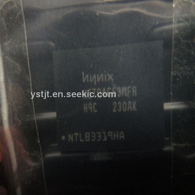

Product Summary
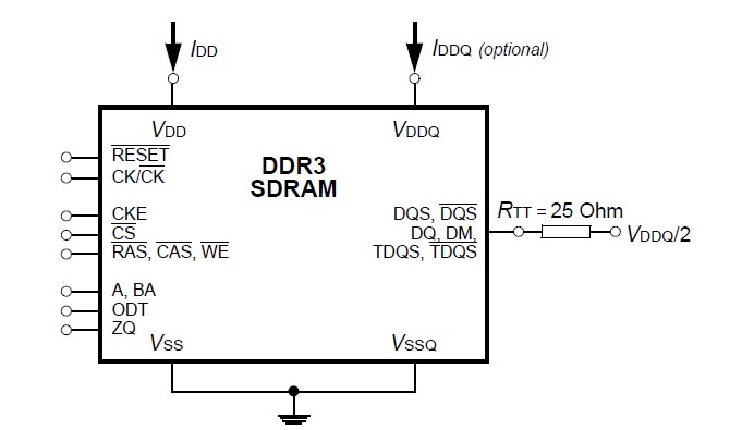
The H5TQ4G63MFR-H9C is a 4Gb CMOS double data rate III (DDR3) synchronous DRAM, ideally suited for the main memory applications which requires large mem-ory density and high bandwidth. SK hynix 4Gb DDR3 SDRAM offer fully synchronous operations refer-enced to both rising and falling edges of the clock. While all addresses and control inputs are latched on the rising edges of the CK (falling edges of the CK), data, data strobes and write data masks inputs are sampled on both rising and falling edges of the H5TQ4G63MFR-H9C. The data paths are internally pipelined and 8-bit prefetched to achieve very high bandwidth.
Parametrics
H5TQ4G63MFR-H9C absolute maximum ratings: (1)VDD, voltage on VDD pin relative to Vss: - 0.4 V ~ 1.80 V; (2)VDDQ, voltage on VDDQ pin relative to Vss: - 0.4 V ~ 1.80 V; (3)VIN, VOUT, voltage on any pin relative to Vss: - 0.4 V ~ 1.80 V; (4)TSTG, storage temperature: -55 to +100 ℃.
Features
H5TQ4G63MFR-H9C features: (1)VDD=VDDQ=1.5V + - 0.075V; (2)Fully differential clock inputs (CK, CK)operation; (3)Differential Data Strobe (DQS, DQS); (4)On chip DLL align DQ, DQS and DQS transition with CK transition; (5)DM masks write data-in at the both rising and falling edges of the data strobe; (6)All addresses and control inputs except data, data strobes and data masks latched on the rising edges of the clock; (7)Programmable CAS latency 6, 7, 8, 9, 10 and 11, 13 supported; (8)Programmable additive latency 0, CL-1, and CL-2 supported; (9)Programmable CAS Write latency (CWL)= 5, 6, 7, 8, 9; (10)Programmable burst length 4/8 with both nibble sequential and interleave mode; (11)BL switch on the fly; (12)8banks.
Diagrams