(China (Mainland))

Product Summary
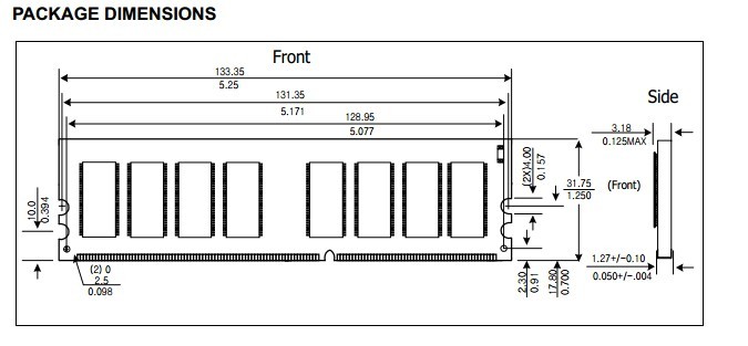
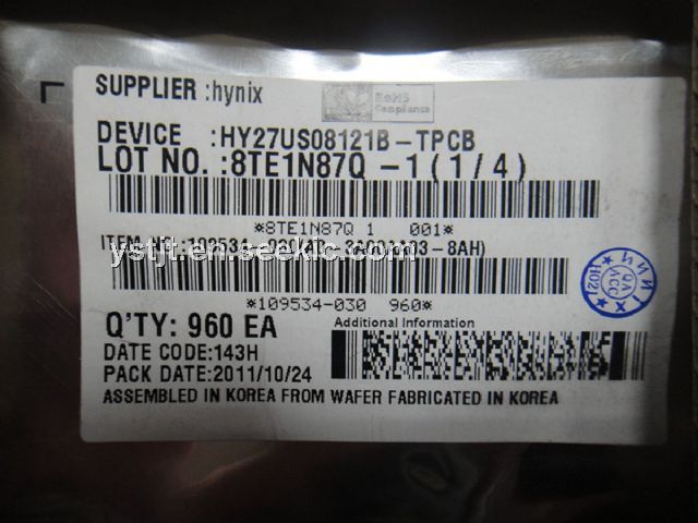
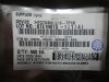
The HY27US08121B-TPCB is an unbuffered 184-pin double data rate Synchronous DRAM Dual In-Line Memory Module(DIMM) which is organized as 32Mx64 high-speed memory arrays. The HY27US08121B-TPCB consists of eight 32Mx8 DDR SDRAM in 400mil TSOP II packages on a 184pin glass-epoxy substrate. The HY27US08121B-TPCB provides a high performance 8-byte interface in 5.25" width form factor of industry standard. It is suitable for easy interchange and addition.
Parametrics
HY27US08121B-TPCB absolute maximum ratings: (1)Power Supply Voltage, VDD: 2.3 to 2.7 V; 2.5V typ; (2)Power Supply Voltage, VDDQ: 2.3 to 2.7 V; 2.5 V typ; (3)Input High Voltage, VIH VREF: + 0.15 to - VDDQ + 0.3 V; (4)Input Low Voltage, VIL: -0.3 to VREF - 0.15 V ; (5)Termination Voltage, VTT: VREF - 0.04 to VREF + 0.04 V; VREF typ; (6)Reference Voltage, VREF: 0.49*VDDQ to 0.51*VDDQ V; 0.5*VDDQ V typ.
Features
HY27US08121B-TPCB features: (1)256MB (32M × 64) Unbuffered DDR DIMM based on 32Mx8 DDR SDRAM; (2)JEDEC Standard 184-pin dual in-line memory module (DIMM); (3)2.5V +/- 0.2V VDD and VDDQ Power supply; (4)All inputs and outputs are compatible with SSTL_2 interface; (5)Fully differential clock operations (CK & /CK) with 100MHz/125MHz/133MHz; (6)All addresses and control inputs except Data, Data strobes and Data masks latched on the rising edges of the clock; (7)Data(DQ), Data strobes and Write masks latched on both rising and falling edges of the clock; (8)Data inputs on DQS centers when write (centered DQ); (9)Data strobes synchronized with output data for read and input data for write; (10)Programmable CAS Latency 2 / 2.5 supported; (11)Programmable Burst Length 2 / 4 / 8 with both sequential and interleave mode; (12)tRAS Lock-out function supported; (13)Internal four bank operations with single pulsed RAS; (14)Auto refresh and self refresh supported; (15)8192 refresh cycles / 64ms.
Diagrams