(China (Mainland))

Product Summary
The K4T1G164QA-ZCD5 is a 1Gb DDR2 SDRAM organized as a 32Mbit x 4 I/Os x 8 banks, 16Mbit x 8 I/Os x 8banks or 8Mbit x 16 I/Os x 8 banks device. This synchronous device achieves high speed double-data-rate transfer rates of up to 667Mb/sec/pin (DDR2-667) for general applications. The K4T1G164QA-ZCD5 is designed to comply with the following key DDR2 SDRAM features such as posted CAS with additive latency, write latency = read latency -1, Off-Chip Driver(OCD) impedance adjustment and On Die Termination.
Parametrics
K4T1G164QA-ZCD5 absolute maximum ratings: (1)VDD, Voltage on VDD pin relative to VSS: -1.0 V to 2.3 V; (2)VDDQ, Voltage on VDDQ pin relative to VSS: -0.5 V to 2.3 V; (3)VDDL, Voltage on VDDL pin relative to VSS: -0.5 V to 2.3 V; (4)VIN, VOUT, Voltage on any pin relative to VSS: -0.5 V to 2.3 V; (5)TSTG, Storage Temperature: -55 to +100℃.
Features
K4T1G164QA-ZCD5 features: (1)JEDEC standard 1.8V ± 0.1V Power Supply; (2)VDDQ = 1.8V ± 0.1V; (3)200 MHz fCK for 400Mb/sec/pin, 267MHz fCK for 533Mb/sec/pin, 333MHz fCK for 667Mb/sec/pin; (4)8 Banks; (5)Posted CAS; (6)Programmable CAS Latency: 3, 4, 5; (7)Programmable Additive Latency: 0, 1 , 2 , 3 and 4; (8)Write Latency(WL) = Read Latency(RL) -1; (9)Burst Length: 4 , 8(Interleave/nibble sequential); (10)Programmable Sequential / Interleave Burst Mode; (11)Bi-directional Differential Data-Strobe (Single-ended data-strobe is an optional feature); (12)Off-Chip Driver(OCD) Impedance Adjustment ; (13)On Die Termination; (14)Special Function Support-PASR(Partial Array Self Refresh); 50ohm ODT; High Temperature Self-Refresh rate enable; (15)Average Refresh Period 7.8us at lower than TCASE; (16)85℃, 3.9us at 85℃ < TCASE < 95℃; (17)Package: 68ball FBGA - 256Mx4/128Mx8 , 84ball FBGA-64Mx16; (18)All of Lead-free products are compliant for RoHS.
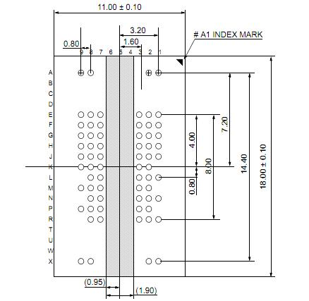
Diagrams