(China (Mainland))

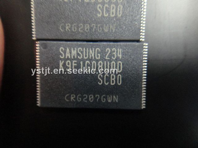
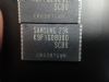
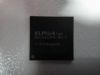
Product Summary
The K9F1G08UOD-SCBO is a 128M x 8 Bit NAND Flash Memory. Its NAND cell provides the most cost-effective solution for the solid state mass storage market. A program operation can be performed in typical 300ms on the 2112-byte page and an erase operation can be performed in typical 2ms on a 128K-byte block. Data in the data page can be read out at 50ns (30ns, K9F1G08U0A) cycle time per byte. The I/O pins serve as the ports for address and data input/output as well as command input. The on-chip write controller automates all program and erase functions including pulse repetition, where required, and internal verification and margining of data. Even the write-intensive systems can take advantage of the K9F1G08UOD-SCBO extended reliability of 100K program/erase cycles by providing ECC(Error Correcting Code) with real time mapping-out algorithm. The K9F1G08UOD-SCBO is an optimum solution for large nonvolatile storage applications such as solid state file storage and other portable applications requiring non-volatility.
Parametrics
K9F1G08UOD-SCBO absolute maximum ratings: (1)Voltage on any pin relative to VSS: -0.6 to + 2.45 V; (2)Temperature Under Bias: -10 to +125 ℃; (3)Storage Temperature: -65 to +150 ℃; (4)Short Circuit Current Ios: 5 mA.
Features
K9F1G08UOD-SCBO features: (1)Voltage Supply: 1.8V device(K9F1G08Q0A): 1.70V~1.95V, 3.3V device(K9F1G08U0A): 2.7 V ~3.6 V; (2)Organization: Memory Cell Array: (128M + 4,096K)bit x 8bit, Data Register: (2K + 64)bit x8bit, Cache Register: (2K + 64)bit x8bit; (3)Automatic Program and Erase: Page Program: (2K + 64)Byte, Block Erase: (128K + 4K)Byte; (4)Page Read Operation: Page Size: 2K-Byte, Random Read: 25ms(Max.), Serial Access: 30ns(Min.): (K9F1G08U0A), 50ns(Min.): (K9F1G08Q0A).
Diagrams