(China (Mainland))


Product Summary
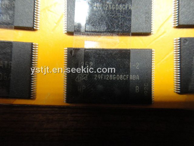
The MT29F128G08CFABAWP is a micron NAND flash device. A target is the unit of memory accessed by a chip enable signal. A target contains one or more NAND Flash die. A NAND Flash die is the minimum unit that can independently execute commands and report status. A NAND Flash die, in the ONFI specification, is referred to as a logical unit (LUN). For further details, see Device and Array Organization. The MT29F128G08CFABAWP additionally includes a synchronous data interface for high-performance I/O operations. When the synchronous interface is active, WE# becomes CLK and RE# becomes W/R#. Data transfers include a bidirectional data strobe (DQS).
Parametrics
MT29F128G08CFABAWP absolute maximum ratings: (1)Voltage input: -0.6 to 4.6 V; (2)VCC supply voltage: -0.6 to 4.6 V; (3)VCCQ supply voltage: -0.6 to 4.6 V; (4)Storage temperature TSTG: -65 to 150 °C.
Features
MT29F128G08CFABAWP features: (1)Open NAND Flash Interface (ONFI) 2.2-compliant; (2)Multiple-level cell (MLC) technology; (3)First block (block address 00h) is valid when shipped from factory; (4)RESET (FFh) required as first command after poweron; (5)Operation status byte provides software method for detecting; (6)Data strobe (DQS) signals provide a hardware method for synchronizing data DQ in the synchronous interface; (7)Copyback operations supported within the plane from which data is read; (8)Quality and reliability; (9)Up to synchronous timing mode 5; (10)Clock rate: 12ns (DDR); (11)Read/write throughput per pin: 50 MT/s; (12)Up to asynchronous timing mode 5; (13)VCC: 2.7-3.6V; (14)VCCQ: 1.7-1.95V, 2.7-3.6V; (15)Page size x8: 8640 bytes (8192 + 448 bytes); (16)Block size: 256 pages (2048K + 112K bytes); (17)Plane size: 2 planes x 2048 blocks per plane.
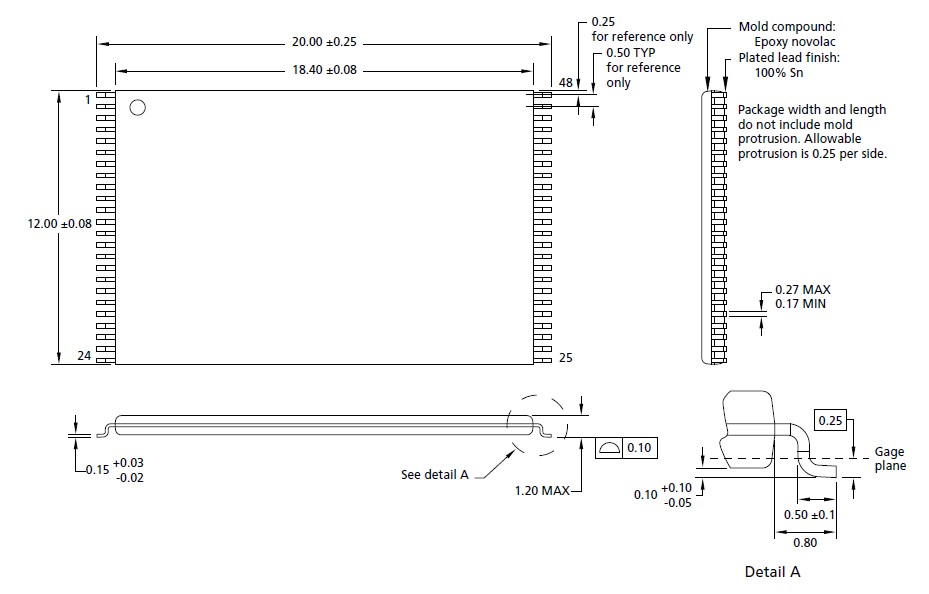
Diagrams