(China (Mainland))


Product Summary
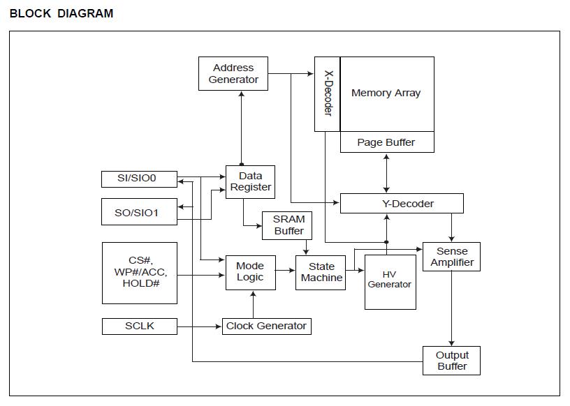
The MX25L5121EOC-20G is a 16,777,216 bit serial Flash memory, which is configured as 2,097,152 x 8 internally. When it is in two I/O read mode, the structure becomes 8,388,608 bits x 2. The MX25L5121EOC-20G features a serial peripheral interface and software protocol allowing operation on a simple 3-wire bus. The three bus signals are a clock input (SCLK), a serial data input (SI), and a serial data output (SO). Serial access to the MX25L5121EOC-20G is enabled by CS# input.
Parametrics
MX25L5121EOC-20G absolute maximum ratings: (1)Ambient Operating Temperature: -40℃ to 85℃ for Industrial grade; (2)Storage Temperature: -55℃ to 125℃; (3)Applied Input Voltage: -0.5V to 4.6V; (4)Applied Output Voltage: -0.5V to 4.6V; (5)VCC to Ground Potential: -0.5V to 4.6V.
Features
MX25L5121EOC-20G features: (1)Serial Peripheral Interface compatible -- Mode 0 and Mode 3; (2)16M:16,777,216 x 1 bit structure or 8,388,608 x 2 bits (two I/O read mode) structure, 32M:33,554,432 x 1 bit structure or 16,772,216 x 2 bits (two I/O read mode) structure, 64M:67,108,864 x 1 bit structure or 33,554,432 x 2 bits (two I/O read mode) structure; (3)512 Equal Sectors with 4K byte each (16Mb), 1024 Equal Sectors with 4K byte each (32Mb), 2048 Equal Sectors with 4K byte each (64Mb); (4)32 Equal Blocks with 64K byte each (16Mb), 64 Equal Blocks with 64K byte each (32Mb), 128 Equal Blocks with 64K byte each (64Mb); (5)Single Power Supply Operation: 2.7 to 3.6 volt for read, erase, and program operations; (6)Latch-up protected to 100mA from -1V to Vcc +1V; (7)Low Vcc write inhibit is from 1.5V to 2.5V.
Diagrams