(China (Mainland))

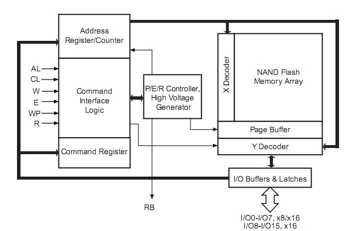
Product Summary
The NAND99R4M2AZBA5F is a NAND Flash Memory. It uses the Single Level Cell (SLC) NAND cell technology. It is referred to as the Small Page family. The NAND99R4M2AZBA5F features an open-drain Ready/Busy output that can be used to identify if the Program/Erase/Read (P/E/R) Controller is currently active. The use of an open-drain output allows the Ready/Busy pins from several memories to be connected to a single pull-up resistor. The NAND99R4M2AZBA5F has the Chip Enable Don’t Care option, which allows the code to be directly downloaded by a microcontroller, as Chip Enable transitions during the latency time do not stop the read operation.
Parametrics
NAND99R4M2AZBA5F absolute maximum ratings: (1)Temperature Under Bias: -50℃ to 125℃; (2)Storage Temperature: -65℃ to 150℃; (3)Lead temperature during soldering: 260℃; (4)Input or Output Voltage: -0.6V to 2.7 V; (5)Supply Voltage: -0.6V to 2.7V.
Features
NAND99R4M2AZBA5F features: (1)high density nand flash memories: Up to 1 Gbit memory array, Up to 32 Mbit spare area, Cost effective solutions for mass storage applications; (2)nand interface: x8 or x16 bus width, Multiplexed Address/Data, Pinout compatibility for all densities; (3)copy back program mode: Fast page copy without external buffering; (4)fast block erase:block erase time: 2ms (Typ); (5)status register; (6)electronic signature; (7)serial number option; (8)Program/Erase locked during Power transitions; (9)100,000 Program/Erase cycles; (10)10 years Data Retention; (11)Lead-Free Components are Compliant with the RoHS Directive; (12)Error Correction Code software and hardware models; (13)Bad Blocks Management and Wear Leveling algorithms; (14)File System OS Native reference software; (15)Hardware simulation models.
Diagrams