(China (Mainland))


Product Summary
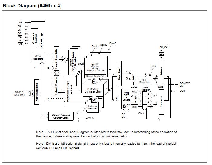
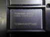
The NT5DS16M16CS-5T is a 256Mb SDRAM device based using a DDR interface. The NT5DS16M16CS-5T is all based on Nanya’s 110 nm design process. The NT5DS16M16CS-5T 256Mb DDR SDRAM uses a double-data-rate architecture to achieve high-speed operation. The double data rate architecture is essentially a 2n prefetch architecture with an interface designed to transfer two data words per clock cycle at the I/O pins. A single read or write access for the NT5DS16M16CS-5T 256Mb DDR SDRAM effectively consists of a single 2n-bit wide, one clock cycle data transfer at the internal DRAM core and two corresponding n-bit wide, one-half-clock-cycle data transfers at the I/O pins.
Parametrics
NT5DS16M16CS-5T absolute maximum ratings: (1)VIN, VOUT, Voltage on I/O pins relative to VSS: -0.5 to VDDQ+ 0.5 V; (2)VIN, Voltage on Inputs relative to VSS: -0.5 to +3.6 V; (3)VDD, Voltage on VDD supply relative to VSS: -0.5 to +3.6 V; (4)VDDQ, Voltage on VDDQ supply relative to VSS: -0.5 to +3.6 V; (5)TA, Operating Temperature (Ambient): 0 to +70 ℃; (6)TSTG, Storage Temperature (Plastic): -55 to +150℃; (7)PD, Power Dissipation: 1.0 W; (8)IOUT, Short Circuit Output Current: 50 mA.
Features
NT5DS16M16CS-5T features: (1)Differential clock inputs (CK and CK); (2)Four internal banks for concurrent operation; (3)Data mask (DM) for write data; (4)DLL aligns DQ and DQS transitions with CK transitions; (5)Commands entered on each positive CK edge; data and data mask referenced to both edges of DQS; (6)Burst lengths: 2, 4, or 8; (7)CAS Latency: 2/2.5(DDR333) , 2.5/3(DDR400); (8)Auto Precharge option for each burst access; (9)Auto Refresh and Self Refresh Modes; (10)7.8μs Maximum Average Periodic Refresh Interval; (11)2.5V (SSTL_2 compatible) I/O; (12)VDD = VDDQ = 2.5V ± 0.2V (DDR333); (13)VDD = VDDQ = 2.6V ± 0.1V (DDR400); (14)Available in Halogen and Lead Free packaging.
Diagrams