(China (Mainland))

Product Summary
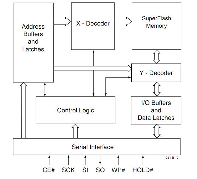
The SST25VF040-80-4I-S2AE is a SPI serial flash memory which features a four-wire, SPI-com-patible interface that allows for a low pin-count package occupying less board space and ultimately lowering total system costs. The SST25VF040-80-4I-S2AE is manufactured with SST’s proprietary, high perfor-mance CMOS SuperFlash Technology. The split-gate cell design and thick-oxide tunneling injector attain better reliability and manufacturability compared with alternate approaches.
Parametrics
SST25VF040-80-4I-S2AE absolute maximum ratings: (1)Temperature Under Bias: -55℃ to +125℃; (2)Storage Temperature: -65℃ to +150℃; (3)D. C. Voltage on Any Pin to Ground Potential: -0.5V to VDD+0.5V; (4)Transient Voltage (<20 ns) on Any Pin to Ground Potential: -2.0V to VDD+2.0V; (5)Package Power Dissipation Capability (Ta = 25℃): 1.0W; (6)Surface Mount Lead Soldering Temperature (3 Seconds): 240℃; (7)Output Short Circuit Current: 50 mA.
Features
SST25VF040-80-4I-S2AE features: (1)Single 2.7-3.6V Read and Write Operations; (2)Serial Interface Architecture, SPI Compatible: Mode 0 and Mode 3; (3)20 MHz Max Clock Frequency; (4)Superior Reliability, Endurance: 100,000 Cycles (typical); Greater than 100 years Data Retention; (5)Low Power Consumption: Active Read Current: 7 mA (typical); Standby Current: 8 μA (typical); (6)Flexible Erase Capability, Uniform 4 KByte sectors; Uniform 32 KByte overlay blocks; (7)Fast Erase and Byte-Program: Chip-Erase Time: 70 ms (typical); Sector- or Block-Erase Time: 18 ms (typical); Byte-Program Time: 14 μs (typical); (8)Auto Address Increment (AAI) Programming, Decrease total chip programming time over Byte-Program operations.
Diagrams