(China (Mainland))

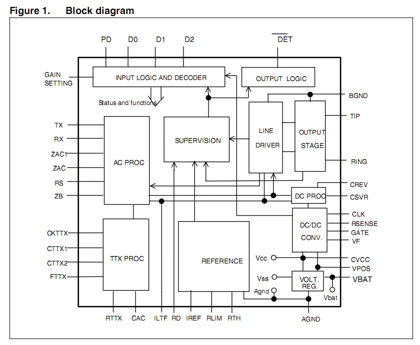
Product Summary
The STLC3055QA7N is a WLL & ISDN-TA subscriber line interface circuit specifically designed for WLL (Wireless Local Loop) and ISDN-Terminal Adaptors. One of the distinctive characteristic of this device is the ability to operate with a single supply voltage (from +5.5V to +15.8V) and self generate the negative battery by means of an on chip DC/DC converter controller that drives an externalMOS switch.
Parametrics
STLC3055QA7N absolute maximum ratings: (1)Positive Supply Voltage: -0.4 to +13 V; (2)AGND to BGND: -1 to +1 V; (3)Pin D0, D1, D2, DET, CKTTX: -0.4 to 5.5 V; (4)Max. junction Temperature: 150℃; (5)Vbtot=|Vpos|+|Vbat|(Total voltage applied to the device supply pins): 90 V; (6)Human body model: ±1750 V; (7)Charged device model: ±500 V.
Features
STLC3055QA7N features: (1)Monochip slic optimised for will and ISDN-TA applications; (2)Implement all key features of the borsht function; (3)Single supply(5.5 to 12V); (4)Built in DC converter controller; (5)On-hook transmission; (6)Programmable off-hook detector threshold; (7)Metering pulse generation and filter; (8)Integrated ringing; (9)Integrated ring trip; (10)Parallel control interface(3.3 V logic level); (11)Programmable constant current feed; (12)Surface mount package; (13)Integrated thermal protection; (14)-40 to +85 ℃ operating range.
Diagrams