(China (Mainland))

Product Summary
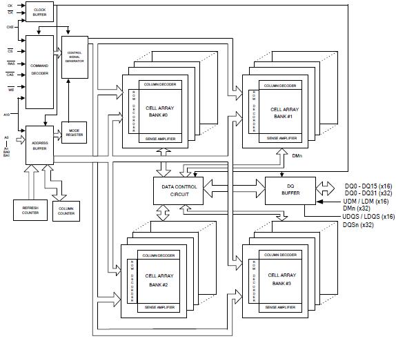
The W948D2FBJX-6E is a high-speed mobile double data rate synchronous dynamic random access memory (LPDDR SDRAM), Using pipelined architecture , An access to the LPDDR SDRAM is burst oriented. Consecutive memory location in one page can be accessed at a burst length of 2, 4, 8 and 16 when a bank and row is selected by an ACTIVE command. Column addresses are automatically generated by the W948D2FBJX-6E internal counter in burst operation. Random column read is also possible by providing its address at each clock cycle.
Parametrics
W948D2FBJX-6E absolute maximum ratings: (1)Voltage on VDD relative to VSS VDD: -0.3 to 2.7 V; (2)Voltage on VDDQ relative to VSS VDDQ: -0.3 to 2.7 V; (3)Voltage on any pin relative to VSS VIN, VOUT: -0.3 to 2.7 V; (4)Operating Case temperature, Tc: -25 to 85℃; -40 to 85℃; (5)Storage Temperature, TSTG: -55 to 150℃; (6)Short Circuit Output Current, IOUT: ±50 mA; (7)Power Dissipation, PD: 1.0 W.
Features
W948D2FBJX-6E features: (1)VDD = 1.7~1.95V; (2)VDDQ = 1.7~1.95V; (3)Data width: x16 / x32; (4)Clock rate: 200MHz(-5),166MHz (-6), 133MHz (-75); (5)Partial Array Self-Refresh(PASR); (6)Auto Temperature Compensated Self-Refresh(ATCSR); (7)Power Down Mode; (8)Deep Power Down Mode (DPD Mode); (9)Programmable output buffer driver strength; (10)Four internal banks for concurrent operation; (11)Data mask (DM) for write data; (12)Clock Stop capability during idle periods; (13)Auto Pre-charge option for each burst access; (14)Double data rate for data output; (15)Differential clock inputs (CK and CK ); (16)Bidirectional, data strobe (DQS); (17)CAS Latency: 2 and 3; (18)Burst Length: 2, 4, 8 and 16; (19)Burst Type: Sequential or Interleave; (20)64 ms Refresh period; (21)Interface: LVCMOS; (22)Support package:; (23)60 balls VFBGA (x16); (24)90 balls VFBGA (x32); (25)Operating Temperature Range; (26)Extended (-25℃ to + 85 ℃); (27)Industrial (-40℃ to + 85 ℃).
Diagrams