(China (Mainland))

Product Summary
The W972GG8JB25I is a 2G bits DDR2 SDRAM, organized as 33,554,432 words × 8 banks × 8 bits. The W972GG8JB25I achieves high speed transfer rates up to 1066Mb/sec/pin (DDR2-1066) for general applications. The W972GG8JB25I is sorted into the following speed grades: -18, -25, 25I and -3. The -18 is compliant to the DDR2-1066 (7-7-7) specification. The -25/25I are compliant to the DDR2-800 (5-5-5) or DDR2-800 (6-6-6) specification (the 25I industrial grade which is guaranteed to support -40°C ≤ TCASE ≤ 95°C). The -3 is compliant to the DDR2-667 (5-5-5) specification. All of the control and address inputs are synchronized with a pair of externally supplied differential clocks. Inputs are latched at the cross point of differential clocks (CLK rising and CLK falling). All I/Os are synchronized with a single ended DQS or differential DQS- DQS pair in a source synchronous fashion.
Parametrics
W972GG8JB25I absolute maximum ratings: (1)Voltage on VDD pin relative to VSS, VDD: -1.0 ~ 2.3 V; (2)Voltage on VDDQ pin relative to VSS, VDDQ: -0.5 ~ 2.3 V; (3)Voltage on VDDL pin relative to VSS, VDDL: -0.5 ~ 2.3 V; (4)Voltage on any pin relative to VSS, VIN, VOUT: -0.5 ~ 2.3 V; (5)Storage temperature, TSTG: -55 ~ 100 °C.
Features
W972GG8JB25I features: (1)Power supply: VDD, VDDQ = 1.8 V ± 0.1 V; (2)Double data rate architecture: two data transfers per clock cycle; (3)CAS latency: 3, 4, 5, 6 and 7; (4)Burst length: 4 and 8; (5)Bi-directional, differential data strobes (DQS and DQS )are transmitted / received with data; (6)Edge-aligned with Read data and center-aligned with Write data; (7)DLL aligns DQ and DQS transitions with clock; (8)Differential clock inputs (CLK and CLK ); (9)Data masks (DM)for write data.; (10)Commands entered on each positive CLK edge, data and data mask are referenced to both edges of DQS; (11)Posted CAS programmable additive latency supported to make command and data bus efficiency; (12)Read latency = Additive latency plus CAS latency (RL = AL + CL); (13)l off-chip-driver impedance adjustment (OCD)and on-die-termination (ODT)for better signal quality; (14)Auto-precharge operation for read and write bursts; (15)Auto refresh and self refresh modes.
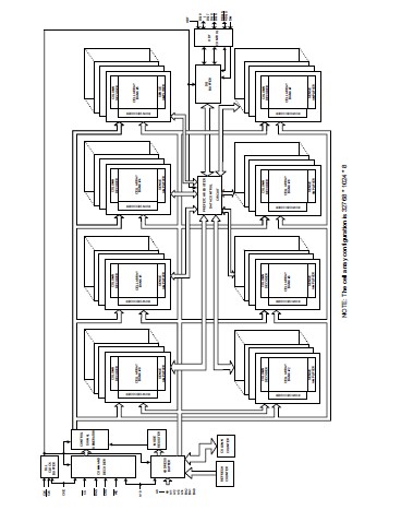
Diagrams