(China (Mainland))

Product Summary
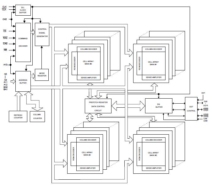
The W9751G6JB-25 is a 512M bits DDR2 SDRAM, organized as 8,388,608 words × 4 banks × 16 bits. This device achieves high speed transfer rates up to 1066Mb/sec/pin (DDR2-1066) for various applications. The W9751G6JB-25 is sorted into the following speed grades: -18, -25, 25I, 25A, 25K and -3. The -18 grade parts is compliant to the DDR2-1066 (7-7-7) specification. The -25/25I/25A/25K grade parts are compliant to the DDR2-800 (5-5-5) or DDR2-800 (6-6-6) specification (the 25I industrial grade parts which is guaranteed to support -40℃ ≤ TCASE ≤ 95℃). The -3 grade parts is compliant to the DDR2-667 (5-5-5) specification.
Parametrics
W9751G6JB-25 absolute maximum ratings: (1)Voltage on VDD pin relative to VSS, VDD: -1.0 ~ 2.3 V; (2)Voltage on VDDQ pin relative to VSS, VDDQ: -0.5 ~ 2.3 V; (3)Voltage on VDDL pin relative to VSS, VDDL: -0.5 ~ 2.3 V; (4)Voltage on any pin relative to VSS, VIN, VOUT: -0.5 ~ 2.3 V; (5)Storage Temperature, TSTG: -55 ~ 150℃.
Features
W9751G6JB-25 features: (1)Power Supply: VDD, VDDQ = 1.8 V ± 0.1V; (2)Double Data Rate architecture: two data transfers per clock cycle; (3)CAS Latency: 3, 4, 5, 6 and 7; (4)Burst Length: 4 and 8; (5)Bi-directional, differential data strobes (DQS and DQS ) are transmitted / received with data; (6)Edge-aligned with Read data and center-aligned with Write data; (7)DLL aligns DQ and DQS transitions with clock; (8)Differential clock inputs (CLK and CLK ); (9)Data masks (DM) for write data; (10)Commands entered on each positive CLK edge, data and data mask are referenced to both edges of DQS; (11)Posted CAS programmable additive latency supported to make command and data bus efficiency; (12)Read Latency = Additive Latency plus CAS Latency (RL = AL + CL); (13)Off-Chip-Driver impedance adjustment (OCD) and On-Die-Termination (ODT) for better signal quality; (14)Auto-precharge operation for read and write bursts; (15)Auto Refresh and Self Refresh modes; (16)Precharged Power Down and Active Power Down; (17)Write Data Mask; (18)Write Latency = Read Latency - 1 (WL = RL - 1); (19)Interface: SSTL_18; (20)Packaged in WBGA 84 Ball (8X12.5 mm2), using Lead free materials with RoHS compliant.
Diagrams