(China (Mainland))

Product Summary
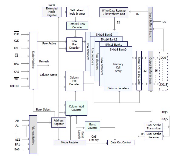
The H5MS5162EER-E3M is a 536,870,912-bit CMOS Low Power Double Data Rate Synchronous DRAM (Mobile DDR SDRAM), ideally suited for mobile applications which use the battery such as PDAs, 2.5G and 3G cellular phones with internet access and multimedia capabilities, mini-notebook, hand-held PCs. It is organized as 4banks of 8,388,608 x16. The H5MS5162EER-E3M uses a double-data-rate architecture to achieve high-speed operation. The double data rate architecture is essentially a 2n prefetch architecture with an interface designed to transfer two data per clock cycle at the I/O pins. The H5MS5162EER-E3M offers fully synchronous operations referenced to both rising and falling edges of the clock. While all address and control inputs are latched on the rising edges of the CK (Mobile DDR SDRAM operates from a differential clock: the crossing of CK going HIGH and CK going LOW is referred to as the positive edge of CK), data, data strobe and data mask inputs are sampled on both rising and falling edges of it (Input data is registered on both edges of DQS, and output data is referenced to both edges of DQS, as well as to both edges of CK). The data paths are internally pipelined and 2-bit prefetched to achieve high bandwidth. All input voltage levels are compatible with LVCMOS.
Parametrics
H5MS5162EER-E3M absolute maximum ratings: (1)Operating Case Temperature TC: -30 ~ 85℃; (2)Storage Temperature TSTG: -55 ~ 150℃; (3)Voltage on Any Pin relative to VSS VIN, VOUT: -0.3 ~ VDDQ+0.3 V; (4)Voltage on VDD relative to VSS VDD: -0.3 ~ 2.7 V; (5)Voltage on VDDQ relative to VSS VDDQ: -0.3 ~ 2.7 V; (6)Short Circuit Output Current IOS: 50 mA; (7)Power Dissipation PD: 0.7 W.
Features
H5MS5162EER-E3M features: (1)Double data rate architecture: two data transfer per clock cycle; (2)Multiplexed Address (Row and Column address); (3)mode rerister set, extended mode register set and status register read; (4)Programmable CAS latency 2 or 3 supported; (5)Programmable burst length 2 / 4 / 8 with both sequential and interleave mode; (6)x16 device: LDQS and UDQS; (7)Bidirectional, data strobe (DQS)is transmitted and received with data, to be used in capturing data at the receiver; (8)Data and data mask referenced to both edges of DQS.
Diagrams