(China (Mainland))

Product Summary
The H5PS1G43EFR-S6C is a 1Gb DDR2 SDRAM.
Parametrics
H5PS1G43EFR-S6C absolute maximum ratings: (1)VDD, Voltage on VDD pin relative to Vss: -1.0 V ~ 2.3 V; (2)VDDQ, Voltage on VDDQ pin relative to Vss: -0.5 V ~ 2.3 V; (3)VDDL, Voltage on VDDL pin relative to Vss: -0.5 V ~ 2.3 V; (4)VIN, VOUT, Voltage on any pin relative to Vss: -0.5 V ~ 2.3 V; (5)TSTG, Storage Temperature: -55 to +100℃; (6)II, Input leakage current; any input 0V VIN VDD; all other balls not under test = 0V): -2 uA ~ 2 uA; (7)IOZ, Output leakage current; 0V VOUT VDDQ; DQ and ODT disabled: -5 uA ~ 5 uA.
Features
H5PS1G43EFR-S6C features: (1)VDD = 1.8 +/- 0.1V; (2)VDDQ = 1.8 +/- 0.1V; (3)All inputs and outputs are compatible with SSTL_18 interface; (4)8 banks; (5)Fully differential clock inputs (CK, /CK) operation; (6)Double data rate interface; (7)Source synchronous-data transaction aligned to bidirectional data strobe (DQS, DQS); (8)Differential Data Strobe (DQS, DQS); (9)Data outputs on DQS, DQS edges when read (edged DQ); (10)Data inputs on DQS centers when write (centered DQ); (11)On chip DLL align DQ, DQS and DQS transition with CK transition; (12)DM mask write data-in at the both rising and falling edges of the data strobe; (13)All addresses and control inputs except data, data strobes and data masks latched on the rising edges of the clock; (14)Programmable CAS latency 3, 4, 5 and 6 supported; (15)Programmable additive latency 0, 1, 2, 3, 4 and 5 supported; (16)Programmable burst length 4/8 with both nibble sequential and interleave mode; (17)Internal eight bank operations with single pulsed RAS; (18)Auto refresh and self refresh supported; (19)tRAS lockout supported; (20)8K refresh cycles /64ms; (21)JEDEC standard 60ball FBGA(x4/x8), 84ball FBGA(x16); (22)Full strength driver option controlled by EMR; (23)On Die Termination supported; (24)Off Chip Driver Impedance Adjustment supported; (25)Read Data Strobe supported (x8 only); (26)Self-Refresh High Temperature Entry.
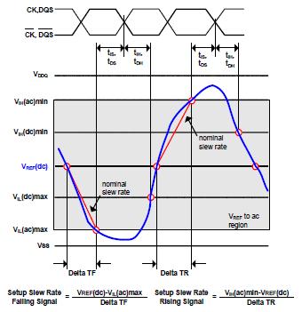
Diagrams