(China (Mainland))

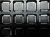
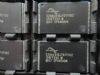
Product Summary
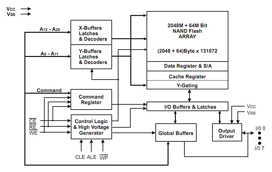
The K9K2G08UOM-PCBO is a 256M x 8 Bit NAND Flash Memory. Its NAND cell provides the most cost-effective solution for the solid state mass storage market. A program operation can be performed in typical 200μs on the 2112 byte page and an erase
operation can be performed in typical 2ms on a 128K-byte block. Data in the data page can be read out at 30ns cycle time per byte. The I/O pins serve as the ports for address and data input/output as well as command input. The on-chip write controller of the K9K2G08UOM-PCBO automates all program and erase functions including pulse repetition, where required, and internal verification and margining of data.
Parametrics
K9K2G08UOM-PCBO absolut maximum ratings: (1)Voltage on any pin relative to VSS, VCC: -0.6 to +4.6V; VIN: -0.6 to +4.6V; VI/O: -0.6 to Vcc+0.3V; (2)Temperature Under Bias, TBIAS: -10 to +125℃; (3)Storage Temperature, TSTG: -65 to +150℃; (4)Short Circuit Current, IOS: 5mA.
Features
K9K2G08UOM-PCBO features: (1)Voltage Supply: -2.7 V ~3.6 V; (2)Organization, Memory Cell Array, (256M + 8,192K)bit x 8bit; Data Register; (2K + 64)bit x8bit; Cache Register; (2K + 64)bit x8bit ; (3)Automatic Program and Erase, Page Program; (2K + 64)Byte; Block Erase, (128K + 4K)Byte; (4)Page Read Operation, Page Size; 2K-Byte, Random Read: 25μs(Max.); Serial Access: 30ns(Min.) 256M x 8 Bit NAND Flash Memory; (5)Fast Write Cycle Time, Program time: 200μs(Typ.); Block Erase Time: 2ms(Typ.), Command/Address/Data Multiplexed I/O Port; (6)Hardware Data Protection, Program/Erase Lockout During Power Transitions; (7)Reliable CMOS Floating-Gate Technology, Endurance: 100K Program/Erase Cycles; Data Retention: 10 Years; (8)Command Register Operation; (9)Cache Program Operation for High Performance Program; (10)Intelligent Copy-Back Operation; (11)Unique ID for Copyright Protection; (12)Package: K9K2G08U0A-VIB0: 48 - Pin WSOP I (12X17X0.7mm); K9K2G08U0A-FIB0: 48 - Pin WSOP I (12X17X0.7mm)- Pb-free Package.
Diagrams