(China (Mainland))


Product Summary
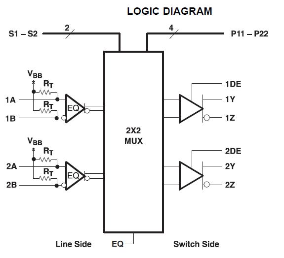
The LVCP40 is a 2x2 non-blocking crosspoint switch in a flow-through pin-out allowing for ease in PCB layout. VML signaling is used to achieve a high-speed data throughput while using low power. Each of the output drivers includes a 2:1 multiplexer to allow any input to be routed to any output. Internal signal paths are fully differential to achieve the high signaling speeds while maintaining low signal skews. The applications of the LVCP40 include Clock Buffering/Clock MUXing, Wireless Base Stations, High-Speed Network Routing, Telecom/Datacom, XAUI 802.3ae Protocol Backplane Redundancy.
Parametrics
LVCP40 absolute maximum ratings: (1)VCC, Supply voltage range: -0.5 V to 6 V; (2)VI, Voltage range, Control inputs, all outputs: -0.5 V to (VCC + 0.5 V); Receiver inputs: -0.5 V to 4 V; (3)ESD, Human Body Model(3), All pins: 4 kV; Charged-Device Model All pins: 500 V; (4)TJ, Maximum junction temperature: See Package Thermal Characteristics Table; (5)Moisture sensitivity level: 2; (6)Reflow temperature package soldering, 4 seconds: 260℃.
Features
LVCP40 features: (1)Up to 4.25 Gbps Operation; (2)Non-blocking Architecture Allows Each Output to be Connected to Any Input; (3)30 ps of Deterministic Jitter; (4)Selectable Transmit Pre-Emphasis Per Lane; (5)Receive Equalization; (6)Available Packaging 24 Pin QFN; (7)Propagation Delay Times: 500 ps Typical; (8)Inputs Electrically Compatible With CML Signal Levels; (9)Operates From a Single 3.3-V Supply; (10)Ability to 3-STATE Outputs; (11)Low Power: 290 mW (typ); (12)Integrated Termination Resistors.
Diagrams