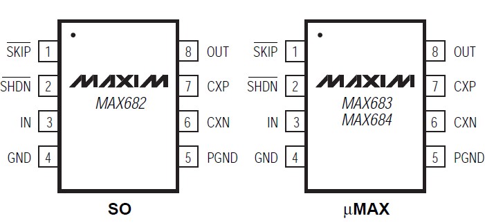
Product Summary
The MAX682ESA is a charge-pump regulator. This device can be used in (1)Flash Memory Supplies; (2)Battery-Powered Applications; (3)Miniature Equipment; (4)PCMCIA Cards; (5)3.3V to 5V Local Conversion Applications; (6)Backup-Battery Boost Converters; (7)3V to 5V GSM SIMM Cards. And it is offered in a spacesaving 8-pin μMAX package that is only 1.1mm high, while the MAX682 is available in an 8-pin SSOP.
Parametrics
MAX682ESA absolute maximum ratings: (1)IN, OUT, SHDN, SKIP to GND: -0.3V to +6V; (2)PGND to GND: ±0.3V; (3)CXN to GND: -0.3V to (VIN + 0.3V); (4)CXP to GND: -0.3V to (VOUT + 0.3V); (5)Output Short-Circuit Duration: 5sec; (6)Storage Temperature Range: -65°C to +160°C; (7)Lead Temperature (soldering, 10s): +300°C; (8)Continuous Power Dissipation 8-Pin SO: 471mW.
Features
MAX682ESA features: (1)Ultra-Small: 1uF Capacitors per 100mA of Output Current; (2)No Inductors Required; (3)Up to 250mA Output Current (MAX682); (4)Regulated 4% Output Voltage; (5)50kHz to 2MHz Adjustable Switching Frequency; (6)2.7V to 5.5V Input Voltage; (7)100uA Quiescent Current in Pulse-Skipping Mode; (8)0.1uA Shutdown Current.
Diagrams

| Image | Part No | Mfg | Description |  |
Pricing (USD) |
Quantity | ||||||||||||
|---|---|---|---|---|---|---|---|---|---|---|---|---|---|---|---|---|---|---|
 |
 MAX682ESA+T |
 Maxim Integrated Products |
 Charge Pumps 3.3VIn to Reg 5Vout Charge Pump |
 Data Sheet |

|
|
||||||||||||
 |
 MAX682ESA-T |
 Maxim Integrated Products |
 Charge Pumps 3.3VIn to Reg 5Vout Charge Pump |
 Data Sheet |
 Negotiable |
|
||||||||||||
 |
 MAX682ESA+ |
 Maxim Integrated Products |
 Charge Pumps 3.3VIn to Reg 5Vout Charge Pump |
 Data Sheet |

|
|
||||||||||||
 |
 MAX682ESA |
 Maxim Integrated Products |
 Charge Pumps 3.3VIn to Reg 5Vout Charge Pump |
 Data Sheet |
 Negotiable |
|
||||||||||||
 (China (Mainland))


