(China (Mainland))

Product Summary
The MT29F16G08ABCBBH1-12ES:B is a micron NAND flash device. A target is the unit of memory accessed by a chip enable signal. A target contains one or more NAND Flash die. A NAND Flash die is the minimum unit that can independently execute commands and report status. A NAND Flash die, in the ONFI specification, is referred to as a logical unit (LUN). For further details, see Device and Array Organization. The MT29F16G08ABCBBH1-12ES:B additionally includes a synchronous data interface for high-performance I/O operations. When the synchronous interface is active, WE# becomes CLK and RE# becomes W/R#. Data transfers include a bidirectional data strobe (DQS).
Parametrics
MT29F16G08ABCBBH1-12ES:B absolute maximum ratings: (1)Voltage input: -0.6 to 4.6 V; (2)VCC supply voltage: -0.6 to 4.6 V; (3)VCCQ supply voltage: -0.6 to 4.6 V; (4)Storage temperature TSTG: -65 to 150 °C.
Features
MT29F16G08ABCBBH1-12ES:B features: (1)Open NAND Flash Interface (ONFI) 2.1-compliant; (2)Single-level cell (SLC) technology; (3)Page size x8: 4320 bytes (4096 + 224 bytes); (4)Block size: 128 pages (512K +28K bytes); (5)Plane size: 2 planes x 2048 blocks per plane; (6)First block (block address 00h) is valid when shipped from factory; (7)RESET (FFh) required as first command after poweron; (8)Operation status byte provides software method for detecting; (9)Data strobe (DQS) signals provide a hardware method for synchronizing data DQ in the synchronous interface; (10)Copyback operations supported within the plane from which data is read; (11)Data retention: 10 years; (12)Endurance: 100,000 PROGRAM/ERASE cycles; (13)Command set: ONFI NAND Flash Protocol; (14)Read cache random, One-time programmable (OTP) mode, Multi-plane commands, Multi-LUN operations, Read unique ID, Copyback.
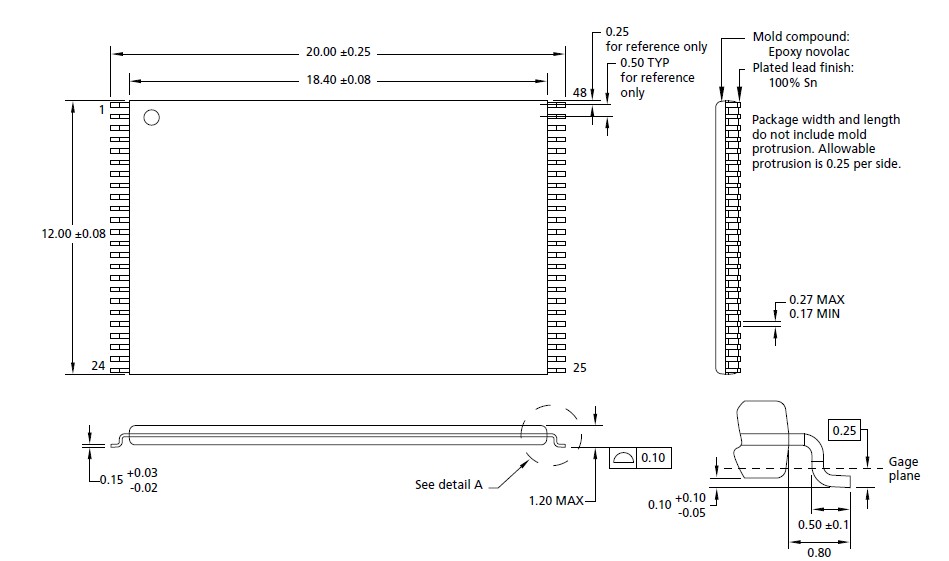
Diagrams