Product Summary
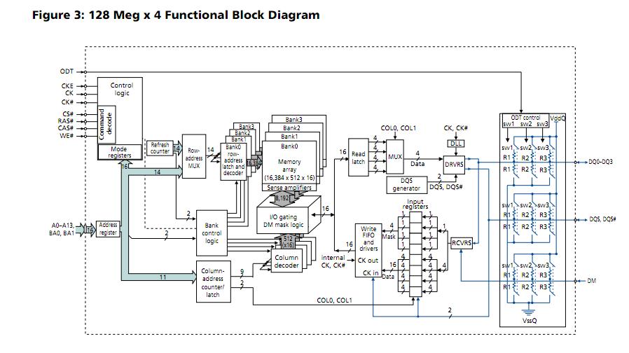
The MT47H32M16HR-3:F D9JLR is a DDR2 SDRAM. The MT47H32M16HR-3:F D9JLR uses a double data rate architecture to achieve high-speed operation. The double data rate architecture is essentially a 4n-prefetch architecture, with an interface designed to transfer two data words per clock cycle at the I/O balls. A single read or write access for the MT47H32M16HR-3:F D9JLR effectively consists of a single 4n-bit-wide, one-clock-cycle data transfer at the internal DRAM core and four corresponding n-bit-wide, one-half-clock-cycle data transfers at the I/O balls.
Parametrics
MT47H32M16HR-3:F D9JLR absolute maximum ratings: (1)Vdd supply voltage relative to Vss, Vdd: –1.0 to 2.3 V; (2)VddQ supply voltage relative to VssQ, VddQ: –0.5 to 2.3 V; (3)VddL supply voltage relative to VssL, VddL: –0.5 to 2.3 V; (4)Voltage on any ball relative to Vss, Vin, Vout: –0.5 to 2.3 V; (5)Input leakage current; any input 0V ≤ Vin ≤ Vdd; all other balls not under test = 0V, Ii: –5 to 5 μA; (6)Output leakage current; 0V ≤ Vout ≤ VddQ; DQ and ODT disabled, Ioz: –5 to 5 μA; (7)Vref leakage current; Vref = valid Vref level, Ivref: –2 to 2 μA.
Features
MT47H32M16HR-3:F D9JLR features: (1)Vdd = +1.8V ±0.1V, VddQ = +1.8V ±0.1V; (2)JEDEC-standard 1.8V I/O (SSTL_18-compatible); (3)Differential data strobe (DQS, DQS#) option; (4)4n-bit prefetch architecture; (5)Duplicate output strobe (RDQS) option for x8; (6)DLL to align DQ and DQS transitions with CK; (7)4 internal banks for concurrent operation; (8)Programmable CAS latency (CL); (9)Posted CAS additive latency (AL); (10)WRITE latency = READ latency - 1 tCK; (11)Selectable burst lengths: 4 or 8; (12)Adjustable data-output drive strength; (13)64ms, 8,192-cycle refresh; (14)On-die termination (ODT); (15)Industrial temperature (IT) option; (16)Automotive temperature (AT) option; (17)RoHS compliant; (18)Supports JEDEC clock jitter specification.
Diagrams

 (China (Mainland))


