(China (Mainland))


Product Summary
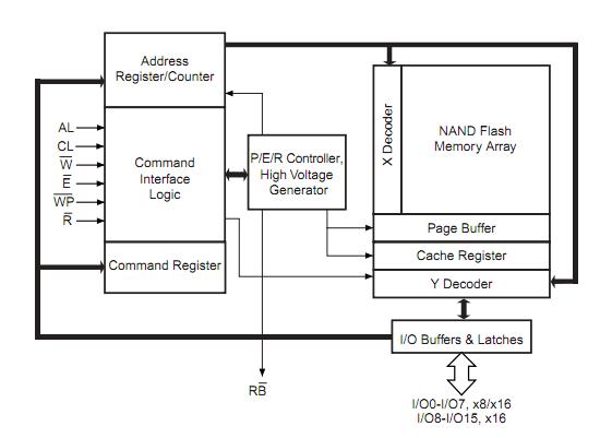
The NAND02GR3B2CZA6E is a non-volatile Flash memory that uses NAND cell technology. The devices range from 1 Gbit to 2 Gbits and operate with either a 1.8V or 3V voltage supply. The size of a Page is either 2112 Bytes (2048 + 64 spare) or 1056 Words (1024 + 32 spare) depending on whether the device has a x8 or x16 bus width. The address lines are multiplexed with the Data Input/Output signals on a multiplexed x8 or x16 Input/Output bus. This interface reduces the pin count and makes the NAND02GR3B2CZA6E possible to migrate to other densities without changing the footprint.
Parametrics
NAND02GR3B2CZA6E absolute maximum ratings: (1)TBIAS, Temperature Under Bias: -50 to 125℃; (2)TSTG, Storage Temperature: -65 to 150℃; (3)VIO, Input or Output Voltage, 1.8V devices: -0.6 to 2.7 V; 3 V devices: -0.6 to 4.6 V; (4)VDD Supply Voltage, 1.8V devices: -0.6 to 2.7 V; 3 V devices: -0.6 to 4.6 V.
Features
NAND02GR3B2CZA6E features: (1)High Density NAND Flash memories, Up to 2 Gbit memory array; Cost effective solutions for mass storage applications; (2)NAND interface, x8 or x16 bus width; Multiplexed Address/ Data; Pinout compatibility for all densities; (3)Supply voltage: 1.8V/3.0V; (4)Page size, x8 device: (2048 + 64 spare) Bytes; x16 device: (1024 + 32 spare) Words; (5)Block size, x8 device: (128K + 4K spare) Bytes; x16 device: (64K + 2K spare) Words; (6)Page Read/Program, Random access: 25μs (max); Sequential access: 30ns (min); Page program time: 200μs (typ); (7)Copy Back Program mode; (8)Cache Program and Cache Read modes; (9)Fast Block Erase: 2ms (typ); (10)Status Register; (11)Electronic Signature; (12)Chip Enable don’t care.
Diagrams