(China (Mainland))


Product Summary
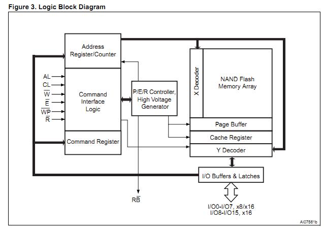
The NAND1GW3B2C2A6 is a non-volatile Flash memory that uses NAND cell technology. The NAND1GW3B2C2A6 ranges from 128Mbits to 1Gbit and operate with either a 1.8V or 3V voltage supply. The size of a Page is either 528 Bytes (512 + 16 spare) or 264 Words (256 + 8 spare) depending on whether the NAND1GW3B2C2A6 has a x8 or x16 bus width. The address lines are multiplexed with the Data In- put/Output signals on a multiplexed x8 or x16 In-put/Output bus. This interface reduces the pin count and makes it possible to migrate to other densities without changing the footprint.
Parametrics
NAND1GW3B2C2A6 absolute maximum ratings: (1)TBIAS, Temperature Under Bias: -50 to 125℃; (2)TSTG, Storage Temperature: -65 to 150℃; (3)VIO, Input or Output Voltage, 1.8V devices: -0.6 to 2.7 V; 3 V devices: -0.6 to 4.6 V; (4)VDD, Supply Voltage, 1.8V devices: -0.6 to 2.7 V; 3 V devices: -0.6 to 4.6 V.
Features
NAND1GW3B2C2A6 features: (1)high density nand flash memories: Up to 1 Gbit memory array; Up to 32 Mbit spare area; Cost effective solutions for mass storage applications; (2)NAND interface: x8 or x16 bus width; Multiplexed Address/ Data; Pinout compatibility for all densities; (3)supply voltage, 1.8V device: VDD = 1.7 to 1.95V; 3.0V device: VDD = 2.7 to 3.6V; (4)page size, x8 device: (512 + 16 spare) Bytes; x16 device: (256 + 8 spare) Words; (5)block size, x8 device: (16K + 512 spare) Bytes; x16 device: (8K + 256 spare) Words; (6)page read / program, Random access: 12μs (max); Sequential access: 50ns (min); Page program time: 200μs (typ); (7)copy back program mode: Fast page copy without external buffering; (8)fast block erase, Block erase time: 2ms (Typ).
Diagrams