(China (Mainland))

Product Summary
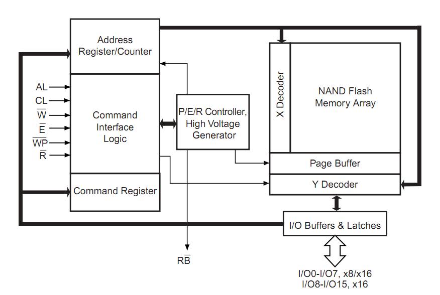
The NAND512R3A2D2A6 is an NAND Flash 528 Byte/ 264 Word Page memory that uses the Single Level Cell (SLC) NAND cell technology. It is referred to as the Small Page family. The NAND512R3A2D2A6 ranges from 128Mbits to 1Gbit and operate with either a 1.8V or 3V voltage supply. The size of a Page is either 528 Bytes (512 + 16 spare) or 264 Words (256 + 8 spare) depending on whether the device has a x8 or x16 bus width.
Parametrics
NAND512R3A2D2A6 absolute maximum ratings: (1)TBIAS, Temperature under bias: -50 to 125℃; (2)TSTG, Storage temperature: -65 to 150℃; (3)VIO, Input or output voltage: -0.6 to 4.6 V; (4)VDD, Supply voltage: -0.6 to 4.6 V.
Features
NAND512R3A2D2A6 features: (1)High density NAND Flash Memory, Up to 8 Gbit memory array; Cost-effective solution for mass storage applications; (2)NAND interface, x8 or 16x bus width; Multiplexed address/data; (3)Supply voltage: 1.8 V or 3.0 V device; (4)Page size, x8 device: (2048 + 64 spare) bytes; x16 device: (1024 + 32 spare) words; (5)Block size, x8 device: (128K + 4 K spare) bytes; x16 device: (64K + 2 K spare) words; (6)Multiplane architecture, Array split into two independent planes; Program/erase operations can be performed on both planes at the same time; (7)Page read/program, Random access: 25 μs (max); Sequential access: 25 ns (min); Page program time: 200 μs (typ); Multiplane page program time (2 pages): 200 μs (typ); (8)Copy back program with automatic error detection code (EDC); (9)Cache read mode; (10)Fast block erase, Block erase time: 1.5 ms (typ); Multiblock erase time (2 blocks): 1.5 ms (typ); (11)Status Register; (12)Electronic signature; (13)Chip Enable don’t care; (14)Serial number option.
Diagrams