(China (Mainland))

Product Summary
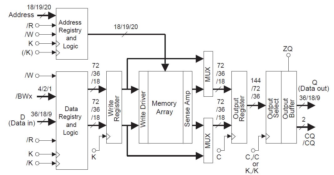
The R1Q3A3618BBG-50R is a 2,097,152-word by 18-bit synchronous quad data rate static RAM fabricated with advanced CMOS technology using full CMOS six-transistor memory cell. The R1Q3A3618BBG-50R integrates unique synchronous peripheral circuitry and a burst counter. All input registers controlled by an input clock pair (K and /K) and are latched on the positive edge of K and /K.
Parametrics
R1Q3A3618BBG-50R absolute maximum ratings: (1)Input voltage on any ball VIN: -0.5 to VDD + 0.5 (2.5 V max.) V; (2)Input/output voltage VI/O: -0.5 to VDDQ + 0.5 (2.5 V max.) V; (3)Core supply voltage VDD: -0.5 to 2.5 V; (4)Output supply voltage VDDQ: -0.5 to VDD V; (5)Junction temperature Tj: +125 (max)℃; (6)Storage temperature TSTG: -55 to +125℃.
Features
R1Q3A3618BBG-50R features: (1)1.8 V ±0.1 V power supply for core (VDD); (2)1.4 V to VDD power supply for I/O (VDDQ); (3)DLL circuitry for wide output data valid window and future frequency scaling; (4)Separate independent read and write data ports with concurrent transactions; (5)100% bus utilization DDR read and write operation; (6)Four-tick burst for reduced address frequency; (7)Two input clocks (K and /K) for precise DDR timing at clock rising edges only; (8)Two output clocks (C and /C) for precise flight time and clock skew matching-clock and data delivered together to receiving device; (9)Internally self-timed write control; (10)Clock-stop capability with restart; (11)User programmable impedance output; (12)Fast clock cycle time: 3.3 ns (300 MHz)/4.0 ns (250 MHz)/ 5.0 ns (200 MHz)/6.0 ns (167 MHz); (13)Simple control logic for easy depth expansion; (14)JTAG boundary scan.
Diagrams