(China (Mainland))

Product Summary
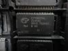
The TC58DVM82F1TGI0BBH is a 128-Mbit (138,412,032) bit NAND Electrically Erasable and Programmable Read-Only Memory (NAND E2PROM) organized as 528 bytes/264 words × 32 pages × 1024 blocks. The device uses dual power supplies (2.7 V to 3.6 V for VCC and 1.65 V to 1.95 V for VCCQ). The TC58DVM82F1TGI0BBH has a 528-byte/264-words static register which allows program and read data to be transferred between the register and the memory cell array in 528-byte/256-words increments. The Erase operation is implemented in a single block unit (16 Kbytes × 512 bytes: 528 bytes × 32 pages/8k words + 256 words: 264 words x 32 pages).
Parametrics
TC58DVM82F1TGI0BBH absolute maximum ratings: (1)VCC, Power Supply Voltage: -0.6~4.6V; (2)VCCQ, I/O port Power Supply Voltage: -0.6~4.6V; (3)VIN, Input Voltage for Control pins: -0.6~4.6V; (4)VI/O, Input/Output Voltage for I/O pins: -0.6 V~VCCQ +0.3 V (≤ 4.6 V); (5)PD, Power Dissipation: 0.3 W; (6)Tsolder, Soldering Temperature(10s): 260℃; (7)Tstg, Storage Temperature: -55 to 150℃; (8)Topr, Operating Temperature: 0~70℃.
Features
TC58DVM82F1TGI0BBH features: (1)Organization, Memory cell allay: 528 × 32K × 8; Register: 528 × 8; Page size: 528 bytes; Block size: (16K × 512); (2)Modes, Read, Reset, Auto Page Program; Auto Block Erase, Status Read; (3)Mode control, Serial input/output; Command control; (4)Power supply, TC58DVM72x1xxxx TC58DAM72x1xxxx, Vcc: 2.7V to 3.6V 2.7V to 3.6V; Vccq: 2.7V to 3.6V 1.65V to 1.95V; (5)Program/Erase Cycles 1E5 cycle (with ECC); (6)Access time, Cell array to register 25μs max; Serial Read Cycle 50 ns min.
Diagrams