(China (Mainland))

Product Summary
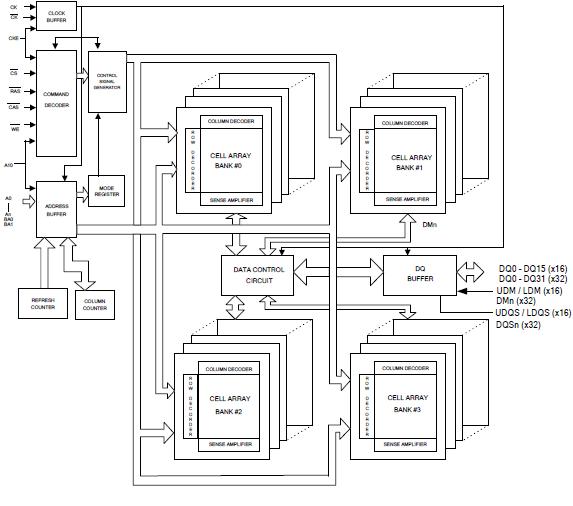
The W948D2FBJX6E is a high-speed mobile double data rate synchronous dynamic random access memory (LPDDR SDRAM), Using pipelined architecture, An access to the LPDDR SDRAM is burst oriented. Consecutive memory location in one page can be accessed at a burst length of 2, 4, 8 and 16 when a bank and row is selected by an ACTIVE command. Column addresses are automatically generated by the LPDDR SDRAM internal counter in burst operation. Random column read of the W948D2FBJX6E is also possible by providing its address at each clock cycle.
Parametrics
W948D2FBJX6E absolute maximum ratings: (1)Voltage on VDD relative to VSS VDD: -0.3 to 2.7 V; (2)Voltage on VDDQ relative to VSS VDDQ: -0.3 to 2.7 V; (3)Voltage on any pin relative to VSS VIN, VOUT: -0.3 to 2.7 V; (4)Operating Case temperature: Tc -25 to 85℃; -40 to 85℃; (5)Storage Temperature, TSTG: -55 to 150℃; (6)Short Circuit Output Current, IOUT: ±50 mA; (7)Power Dissipation, PD: 1.0 W.
Features
W948D2FBJX6E features: (1)VDD = 1.7~1.95V; (2)VDDQ = 1.7~1.95V; (3)Data width: x16 / x32; (4)Clock rate: 200MHz(-5),166MHz (-6), 133MHz (-75); (5)Partial Array Self-Refresh(PASR); (6)Auto Temperature Compensated Self-Refresh(ATCSR); (7)Power Down Mode; (8)Deep Power Down Mode (DPD Mode); (9)Programmable output buffer driver strength; (10)Four internal banks for concurrent operation; (11)Data mask (DM) for write data; (12)Clock Stop capability during idle periods; (13)Auto Pre-charge option for each burst access; (14)Double data rate for data output; (15)Differential clock inputs (CK and CK ); (16)Bidirectional, data strobe (DQS); (17)CAS Latency: 2 and 3; (18)Burst Length: 2, 4, 8 and 16; (19)Burst Type: Sequential or Interleave; (20)64 ms Refresh period; (21)Interface: LVCMOS; (22)Support package: 60 balls VFBGA (x16); 90 balls VFBGA (x32); (23)Operating Temperature Range, Extended (-25℃ to + 85 ℃); Industrial (-40℃ to + 85 ℃).
Diagrams