Product Summary
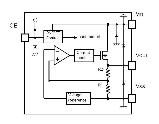
The XC6219B181MR is a highly accurate, low noise, CMOS LDO Voltage Regulator. Offering low output noise, high ripple rejection ratio, low dropout and very fast turn-on times, the XC6219B181MR is ideal for today’s cutting edge mobile phone. Internally the XC6219B181MR includes a reference voltage source, error amplifiers, driver transistors, current limiters and phase compensators. The applications of the XC6219B181MR include Mobile phones, Cordless phones and radio communication equipment, Portable games, Cameras, video cameras, Reference voltage sources, Battery powered equipment.
Parametrics
XC6219B181MR absolute maximum ratings: (1)Input Voltage, VIN: 7.0 V; (2)Output Current, IOUT: 500 mA; (3)Output Voltage, VOUT: VSS -0.3 to VIN + 0.3 V; (4)CE Pin Voltage, VCE: VSS -0.3 to VIN + 0.3 V; (5)Power Dissipation, SOT-25, Pd: 250mW; SOT-89, Pd: 500mW; USP-6B, Pd: 100mW; (6)Operating Temperature Range, Topr: -40 to +85℃; (7)Storage Temperature Range, Tstg: -55 to +125℃.
Features
XC6219B181MR features: (1)CMOS Low Power Consumption; (2)Dropout Voltage 60mV @ 30mA; 200mV @ 100mA; (3)Output Current 150mA (VOUT<1.75V); 240mA (VOUT>1.8V); (300mA limit); (4)Highly Accurate, +2%, (+30mV when VOUT>1.5V); (5)Output Voltage Range 0.9V to 5.0V (50mV increments); (6)Low ESR Ceramic Capacitor Compatible.
Diagrams

 (China (Mainland))


